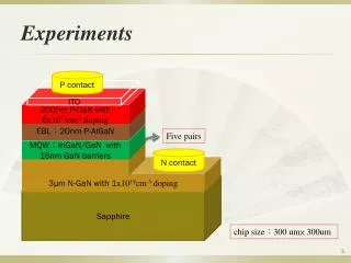
Experiments
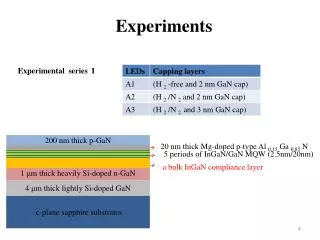
Experiments. Experimental series I. 200 nm thick p- GaN. 20 nm thick Mg-doped p-type Al 0.15 Ga 0.85 N. 5 periods of InGaN/GaN MQW (2.5nm/20nm). a bulk InGaN compliance layer. 1 μ m thick heavily Si-doped n- GaN. 4 μ m thick lightly Si-doped GaN. c-plane sapphire substrates.

Experiments
E N D
Presentation Transcript
Experiments Experimental series I 200 nm thick p-GaN 20 nm thick Mg-doped p-type Al 0.15 Ga 0.85 N 5 periods of InGaN/GaN MQW (2.5nm/20nm) a bulk InGaN compliance layer 1 μm thick heavily Si-doped n-GaN 4 μm thick lightly Si-doped GaN c-plane sapphire substrates
Experimental series II 200 nm thick p-GaN 20 nm thick Mg-doped p-type Al 0.15 Ga 0.85 N 5 periods of InGaN/GaN MQW (2.5nm/20nm) 20 periods of InGaN/GaN strained superlattice compliance layer 1 μm thick heavily Si-doped n-GaN 4 μm thick lightly Si-doped GaN Capping layers :B0=A2 Superlatticebetter then InGaN bulk layer at 0.5mA :LOP enhancement ~25% c-plane sapphire substrates