Detectors
Detectors. RIT Course Number 1051-465 Lecture Circuits. Aims for this lecture. describe basic circuits used in modern detectors and associated electronics systems give detailed examples of readout circuits in common usage today. Lecture Outline. kinds of circuits source follower


Detectors
E N D
Presentation Transcript
Detectors RIT Course Number 1051-465 Lecture Circuits
Aims for this lecture • describe basic circuits used in modern detectors and associated electronics systems • give detailed examples of readout circuits in common usage today
Lecture Outline • kinds of circuits • source follower • current source • pre-amp • filter • buffer/driver • ADC • readout electronics examples • Leach • SIDECAR ASIC
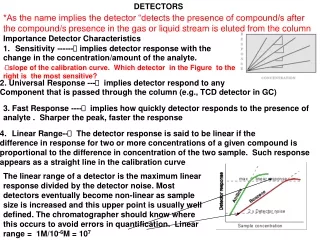
The Purpose of Detector Circuits • Electronic circuits serve the purpose of operating and reading detectors. • Ideally, the electronics would not degrade the signal of interest. • Of course, electronics are “real” devices and are thus imperfect. • Therefore, electronics should carefully be designed and implemented such that non-electronic sources of signal degradation dominate. • As an example, the electronic read noise should be less than the signal shot noise.
Detector Electronics System Block Diagram detector computer (disk/display) ADC readout amp amp cable bias clock
JFET Switch • An ideal switch would make a short-circuit connection when “on” and an open connection when “off.” In other words, it would behave like a mechanical switch. • The following switch quenches current flow when the JFET gate is reverse-biased below the cutoff level.
Vin d g s Vout R1 JFET Switch On state = signal passed ► RDS ~ 25 - 100Ω Off state = open circuit ► RDS ~ 10 GΩ • Vout=Vin when switch is “on” • Vout=0 when switch is “off” • circuit behaves like a voltage divider when on.
linear regime FET Switch Operates in Linear Regime • Switch “off” corresponds to VGS=VGS(off). • Switch “on” corresponds to VGS>VGS(off). • Ideally, RFET is small, i.e. IV slope is large below.
MOSFET Switch • The MOSFET switch is most popular type of switch. • It is good for transmitting low level voltage signals (as opposed to high current). • Output swing depends critically on RD (ID=IDSS for VGS=0). • Current flows at all times.
CMOS Switch • Complementary MOSFET (CMOS) switch is most common. • With this circuit, the output swing spans the full range. • Note the absence of resistors; power is low. • Q1 and Q2 are not “on” at same time -> no current! p-channel (pnp) n-channel (npn)
VDD g s R Source Follower • A “source follower” circuit uses a FET in a circuit in which vs “follows” vg. • It converts the output impedance of a signal from high to low. This is useful for driving long cables with small signals. vs=Rid id=gmvgs=gm(vg-vs) vs=[Rgm/(1+Rgm)]vg gain=vs/vg=1/(1+1/Rgm) So, gain~1 for Rgm>>1. Note that gm is the transconductance, and 1/gm is the output impedance, typically ~a few hundred Ohms. By replacing the resistor with a current source, R~infinite, so gain is nearer to 1.
VDD g s Source Follower with Current Source • By replacing the resistor with a current source, R~infinite, so gain is nearer to 1. • The current source is made of a FET with grounded gate. • This circuit is sometimes referred to as a buffer.
FET Current Source: Schematic • A self-biased FET will deliver a nearly fixed current regardless of load if operated in the saturation region. ideal region for current source
FET Current Source: Biasing • The current source is most stable at VGS just above the cutoff voltage (VGS,off). • The is where the transconductance goes to zero.
FET Current Source: Parts • The following table gives output current versus bias resistance for a variety of parts.
Op-amps • Ideal IC Op-amp has • Infinite voltage gain • Infinite input impedance • Zero output impedance • Infinite bandwidth • Zero input offset voltage (i.e., exactly zero out if zero in). • Golden Rules (Horowitz & Hill) • I. The output attempts to do whatever is necessary to make the voltage difference between the inputs zero. (The Voltage Rule) • II. The inputs draw no current. (The Current Rule)
Op-amps Through History 1952 K2-W tube op-amp GAP Researches, Inc. 1964 uA702 op-amp Fairchild Semiconductor ~$1300 (2009$) 1967 uA709 op-amp Fairchild Semiconductor ~$50 (2009$) • Bob Widlar designed the uA709. He requested a raise from his boss, Charles Sporck, but he was denied. • So, he quit, and went to National Semiconductor. • One year later, Sporck became President of National Semiconductor! • Widlar got his raise and retired in 1970, just before his 30th birthday.
Op-amps: non-inverting amplifier • According to the golden rules, V2=V3, and the current into terminal 2 is zero.
Op-amps: inverting amplifier • According to the golden rules, the current into terminal 2 is zero.
Op-amps: differential amplifier • If all resistors are equal, then the output is the difference. • If R3=R4 and R1=R2, then the output is the amplified difference.
Instrumentation Amplifier • IAs have low noise, high gain, high impedance input.
RC Filter Time Constant A capacitor of capacitance C is initially uncharged. To charge it, we close switch S on point a. This completes an RC series circuit consisting of the capacitor, an ideal battery, and a resistance R. When switch S is closed on a, the capacitor is charged through the resistor. When the switch is afterward closed on b, the capacitor discharges through the resistor. As soon as the circuit is complete, charge flows between a capacitor plate and a battery terminal on each side of the capacitor. This current increases the charge q on the plates and the potential difference VC (= q/C) across the capacitor. When that potential difference equals the potential difference across the battery, the current is zero. The equilibrium (final) charge on the then fully charged capacitor satisfies q = CV. Here we want to examine the charging process. In particular we want to know how the charge q(t) on the capacitor plates, the potential difference VC(t) across the capacitor, and the current i(t) in the circuit vary with time during the charging process. We begin by applying the loop rule to the circuit, traversing it clockwise from the negative terminal of the battery. We find The last term on the left side represents the potential difference across the capacitor. The term is negative because the capacitor's top plate, which is connected to the battery's positive terminal, is at a higher potential than the lower plate. Thus, there is a drop in potential as we move down through the capacitor. Note that Substituting, we find Solving, we find
RC time constant • The RC filter attenuates voltage fluctations. • The gain is f0=1/(2pt)=1/(2pRC).
RC Filter Step Response • Any system with resistance and capacitance will have a slow response to a step function. • This effect limits the speed of switching circuits, i.e. pixel clocking in a detector.
Frequency Limitation of MOSFET • A MOSFET has some capacitance and resistance that limit its frequency response. • Consider a typical example:
Op-amps: buffer • According to the golden rules, V2=V3, so Vout=Vin.
ADCs and DACs • An Analog-to-Digital Converter (ADC) converts an analog signal to a digital signal. • A Digital-to-Analog Converter (DAC) does the opposite.
ADCs and Resolution • Resolution sets the smallest increment that can be measured. • In the water tank analogy, the resolution sets the minimum increment of depth that can be measured.
ADCs • There are a half-dozen or so ADC architectures in common usage. • A flash ADC has a bank of comparators, each firing for their decoded voltage range. The comparator bank feeds a logic circuit that generates a code for each voltage range. Direct conversion is very fast, but usually has only 8 bits of resolution (255 comparators - since the number of comparators required is 2n - 1) or fewer, as it needs a large, expensive circuit. • A successive-approximation ADC uses a comparator to reject ranges of voltages, eventually settling on a final voltage range. Successive approximation works by constantly comparing the input voltage to the output of an internal digital to analog converter (DAC, fed by the current value of the approximation) until the best approximation is achieved. At each step in this process, a binary value of the approximation is stored in a successive approximation register (SAR). • A ramp-compare ADC produces a saw-tooth signal that ramps up, then quickly falls to zero. When the ramp starts, a timer starts counting. When the ramp voltage matches the input, a comparator fires, and the timer's value is recorded. • An integrating ADC (also dual-slope or multi-slope ADC) applies the unknown input voltage to the input of an integrator and allows the voltage to ramp for a fixed time period (the run-up period). Then a known reference voltage of opposite polarity is applied to the integrator and is allowed to ramp until the integrator output returns to zero (the run-down period). • A delta-encoded ADC or Counter-ramp has an up-down counter that feeds a digital to analog converter (DAC). The input signal and the DAC both go to a comparator. The comparator controls the counter. The circuit uses negative feedback from the comparator to adjust the counter until the DAC's output is close enough to the input signal. • A pipeline ADC (also called subranging quantizer) uses two or more steps of subranging. First, a coarse conversion is done. In a second step, the difference to the input signal is determined with a digital to analog converter (DAC). This difference is then converted finer, and the results are combined in a last step. • A Sigma-Delta ADC (also known as a Delta-Sigma ADC) oversamples the desired signal by a large factor and filters the desired signal band. Generally a smaller number of bits than required are converted using a Flash ADC after the Filter. The resulting signal, along with the error generated by the discrete levels of the Flash, is fed back and subtracted from the input to the filter.
Unit Cell Circuit Schematic Φr Vout Φc Vreset +Vbias Vreset Vdrain