Semiconductor Chemistry: Bonds, Structures & Properties
Understand semiconductor chemistry including chemical bonds like covalent, metallic, and ionic, crystal spacing, solid properties, and more. Delve into topics like semiconductor structure, properties, and behavior essential for electronic device operation.

Semiconductor Chemistry: Bonds, Structures & Properties
E N D
Presentation Transcript
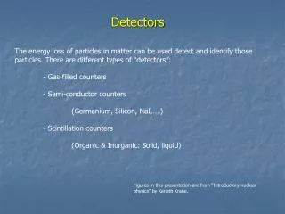
Detectors RIT Course Number 1051-465 Lecture N: Semiconductors
Chemical Bonds • Van der Waals (organic, polymers) • Dipole – hydrogen bond (HF, ice) • Metallic (Fe) • Covalent (silicon, InSb) • Ionic (NaCl)
Types of Solids: Ionic Solid Properties • Formed by Coulombic attraction between ions. • Examples include group I alkali cations paired with group VII halide anions, e.g. Na+ Cl-. • Large cohesive energy (2-4 eV/ atom). • Leads to high melting and boiling points. • Low electrical conductivity. • No “free” electrons to carry current. • Transparent to visible light. • Photon energy too low to “free” electrons. • Soluble in polar liquids like water. • Dipole of water attracts ions.
Crystal Spacing • Potential Energy: Utot = Uattract (+,–) + Urepulse (–, –)
Types of Solids: Example Crystalline Structures Body-Centered Cubic Face-Centered Cubic Simple Cubic FCC structure: NaCl Na+ Cl-
Types of Solids: Covalent Solid • Examples include group IV elements (C, Si) and III-V elements (GaAs, InSb). • Formed by strong, localized bonds with stable, closed-shell structures. • Larger cohesive energies than for ionic solids (4-7 eV/atom). • Leads to higher melting and boiling points. • Low electrical conductivity. • Due to energy band gap that charged carriers must overcome in order to conduct.
Semiconductors are made up of individual atoms bonded together in a regular, periodic structure to form an arrangement whereby each atom is surrounded by 8 electrons. An individual atom consists of a nucleus made up of a core of protons (positively charged particles) and neutrons (particles having no charge) surrounded by electrons. The number of electrons and protons is equal, such that the atom is overall electrically neutral. The electrons occupy certain energy levels, based on the number of electrons in the atom, which is different for each element in the periodic table. The structure of a semiconductor is shown in the figure below. • Schematic representation of covalent bonds in a silicon crystal lattice. • The atoms in a semiconductor are materials from either group IV of the periodic table, or from a combination of group III and group V (called III-V semiconductors), or of combinations from group II and group VI (called II-VI semiconductors). Silicon is the most commonly used semiconductor material as it forms the basis for integrated circuit (IC) chips and is the most mature technology and most solar cells are also silicon based. A full periodic table is given in the page Periodic Table. Several of the material properties of silicon are given in the page Silicon Material Parameters. • Section from the periodic table. More common semiconductor materials are shown in blue. A semiconductor can be either of a single element, such as Si or Ge, a compound, such as GaAs, InP or CdTe, or an alloy, such as SixGe(1-x) or AlxGa(1-x)As, where x is the fraction of the particular element and ranges from 0 to 1. • The bond structure of a semiconductor determines the material properties of a semiconductor. One key effect is limit the energy levels which the electrons can occupy and how they move about the crystal lattice. The electrons surrounding each atom in a semiconductor are part of a covalent bond. A covalent bond consists of two atoms "sharing" a single electron, such that each atom is surrounded by 8 electrons. The electrons in the covalent bond are held in place by this bond and hence they are localised to region surrounding the atom. Since they cannot move or change their energy, electrons in a bond are not considered "free" and cannot participate in current flow, absorption or other physical processes of interest in solar cells. However, only at absolute zero are all electrons in a bonded arrangement. At elevated temperatures, the electron can gain enough energy to escape from its bond, and if this happens, the electron is free to move about the crystal lattice and participate in conduction. At room temperature, a semiconductor has enough free electrons to allow it to conduct current, while at, or close to absolute temperatures, a semiconductor behaves like an insulator. • The presence of the bond introduces two distinct energy states for the electrons. The lowest energy position for the electron is to be in its bound state. However, if the electron has enough thermal energy to break free of its bond, then it becomes free. The electron cannot attain energy values intermediate to these two levels; it is either at a low energy position in the bond, or it has gained enough energy to break free and therefore has a certain minimum energy. This minimum energy is called the "band gap" of a semiconductor. The number and energy of the free electrons is basic to the operation of electronic devices. • The space left behind by the electrons allows a covalent bond to move from one electron to another, thus appearing to be a positive charge moving through the crystal lattice. This empty space is commonly called a "hole", and is similar to an electron, but with a positive charge. • Animation showing formation of "free" electrons and holes when an electron can escape its bond. • The most important parameters of a semiconductor material for solar cell operation are: • the band gap; • the number of free carriers available for conduction; and • the "generation" and recombination of free carriers in response to light shining on the material. • More detail on these properties is given in the following pages.
Types of Solids: Example Crystalline Structures Graphite Planar sp2 bonding (good lubricant) Diamond Tetrahedral sp3 bonding (very hard!) Bond angle = 109.5º
Types of Solids: Metal • Formed by Coulombic attraction between (+) lattice ions and(–) electron “gas.” • Metallic bonds allows electrons to move freely through lattice. • Smaller cohesive energy (1-4 eV). • High electrical conductivity. • Absorbs visible light (non-transparent, “shiny” due to re-emission). • Good alloy formation (due to non-directional metallic bonds).
Solution in periodic lattice Free electron Momentum P= (h/2π)k energy E = (h/2π)²k²/2m
Classical Theory of Conduction (E&M Review) Microscopic Macroscopic • Drift velocityvd is net motion of electrons (0.1 to 10-7 m/s). • Scattering timet is time between electron-lattice collisions.
Mobility • µ = eτ/m = mobility • Key parameter in semiconductors • Limited by ; • Lattice scattering (µ down as temperature up) • Impurity scattering (independent of temperature)
Classical Theory of Conduction: Electron Motion • Electron travels at fast velocities for a time t and then “collides” with the crystal lattice. • Results in a net motion opposite to the E field with drift velocityvd. • Scatter time t decreaseswithincreasing temperature T, i.e. more scattering at higher temperatures (leads to higher resistivity).
Classical Theory of Conduction: Resistivity vs. Temp. • Metal:Resistanceincreases with Temperature. • Why? Temp t, n same (same # conduction electrons) r • Semiconductor: Resistance decreases with Temperature. • Why? Tempt, n (“free-up” carriers to conduct)r
Band Theory: Two Approaches • There are two approaches to finding the electron energies associated with atoms in a periodic lattice. • Approach #1: “Bound” Electron Approach (single atom energies!) • Isolated atoms brought close together to form a solid. • Approach #2: “Unbound” or Free Electron Approach (E = p2/2m) • Free electrons modified by a periodic potential (i.e. lattice ions). • Both approaches result ingrouped energy levels with allowed and forbidden energy regions. • Energy bands overlap for metals. • Energy bands do not overlap (or have a “gap”) for semiconductors.
For the total number Nof atoms in a solid (1023 cm–3), N energy levelssplit apart within a width E. Leads to a band of energiesfor each initial atomic energy level (e.g. 1s energy band for 1s energy level). Band Theory: “Bound” Electron Approach Two atoms Six atoms Solid of N atoms Electrons must occupy different energies due to Pauli Exclusion principle.
Probability of electrons (fermions) to be found at various energy levels. Band Diagram: Fermi-Dirac “Filling” Function • At RT, E – EF = 0.05 eV f(E) = 0.12 E –EF = 7.5 eV f(E) = 10 –129 • Exponential dependence has HUGE effect! • Temperature dependence of Fermi-Dirac function shown as follows: Step function behavior “smears” out at higher temperatures.
Band Diagram: Metal T > 0 • At T = 0, all levels in conduction band below the Fermi energy EF are filled with electrons, while all levels aboveEF areempty. • Electrons are free to move into “empty” states of conduction band with only a small electric field E, leading to high electrical conductivity! • At T > 0, electrons have a probability to be thermally “excited” from below the Fermi energy to above it. EC,V Fermi “filling” function Energy band to be “filled” EF Conduction band (Partially Filled) E = 0
Band Diagram: Insulator Conduction band (Empty) T > 0 • At T = 0, lower valence band is filled with electrons and upper conduction band is empty, leading to zero conductivity. • Fermi energy EF is at midpoint of large energy gap (2-10 eV) between conduction and valence bands. • At T > 0, electrons are usually NOT thermally “excited” from valence to conduction band, leading to zero conductivity. EC Egap EF EV Valence band (Filled)
T > 0 Conduction band (Partially Filled) EC EF EV Valence band (Partially Empty) Band Diagram: Semiconductor with No Dopingaka intrinsic semiconductor • At T = 0, lower valence band is filled with electrons and upper conduction band is empty, leading to zero conductivity. • Fermi energy EF is at midpoint of small energy gap (<1 eV) between conduction and valence bands. • At T > 0, electrons thermally “excited” from valence to conduction band, leading to measurable conductivity. Ni = np function of temperature
For group IV Si, add a group V element to“donate” an electron and make n-type Si (more negative electrons!). “Extra” electron is weakly bound, with donor energy level ED just below conduction band EC. Dopant electrons easily promoted to conduction band, increasing electrical conductivity by increasing carrier density n. Fermi level EF moves up towards EC. n-type Si EC ED EF Egap~ 1 eV EV Band Diagram: Donor Dopant in Semiconductor • Increase the conductivityof a semiconductor by adding a small amount of another material called a dopant (instead of heating it!)
Even though electrons are known to exist in ethereal, “cloud-like” forms of distributed probability rather than as discrete chunks of matter, those “clouds” have other characteristics that are discrete. Any electron in an atom can be described by four numerical measures (the previously mentioned quantum numbers), called the Principal, Angular Momentum, Magnetic, and Spin numbers. The following is a synopsis of each of these numbers' meanings: Principal Quantum Number: Symbolized by the letter n, this number describes the shell that an electron resides in. An electron “shell” is a region of space around an atom's nucleus that electrons are allowed to exist in, corresponding to the stable “standing wave” patterns of de Broglie and Bohr. Electrons may “leap” from shell to shell, but cannot exist between the shell regions. The principle quantum number must be a positive integer (a whole number, greater than or equal to 1). In other words, principle quantum number for an electron cannot be 1/2 or -3. These integer values were not arrived at arbitrarily, but rather through experimental evidence of light spectra: the differing frequencies (colors) of light emitted by excited hydrogen atoms follow a sequence mathematically dependent on specific, integer values as illustrated in Figureprevious. Each shell has the capacity to hold multiple electrons. An analogy for electron shells is the concentric rows of seats of an amphitheater. Just as a person seated in an amphitheater must choose a row to sit in (one cannot sit betweenrows), electrons must “choose” a particular shell to “sit” in. As in amphitheater rows, the outermost shells hold more electrons than the inner shells. Also, electrons tend to seek the lowest available shell, as people in an amphitheater seek the closest seat to the center stage. The higher the shell number, the greater the energy of the electrons in it. The maximum number of electrons that any shell may hold is described by the equation 2n2, where “n” is the principle quantum number. Thus, the first shell (n=1) can hold 2 electrons; the second shell (n=2) 8 electrons, and the third shell (n=3) 18 electrons. (Figure below) Principal quantum number n and maximum number of electrons per shell both predicted by 2(n2), and observed. Orbitals not to scale. Electron shells in an atom were formerly designated by letter rather than by number. The first shell (n=1) was labeled K, the second shell (n=2) L, the third shell (n=3) M, the fourth shell (n=4) N, the fifth shell (n=5) O, the sixth shell (n=6) P, and the seventh shell (n=7) Q. Angular Momentum Quantum Number: A shell, is composed of subshells. One might be inclined to think of subshells as simple subdivisions of shells, as lanes dividing a road. The subshells are much stranger. Subshells are regions of space where electron “clouds” are allowed to exist, and different subshells actually have different shapes. The first subshell is shaped like a sphere, (Figure below(s) ) which makes sense when visualized as a cloud of electrons surrounding the atomic nucleus in three dimensions. The second subshell, however, resembles a dumbbell, comprised of two “lobes” joined together at a single point near the atom's center. (Figure below(p) ) The third subshell typically resembles a set of four “lobes” clustered around the atom's nucleus. These subshell shapes are reminiscent of graphical depictions of radio antenna signal strength, with bulbous lobe-shaped regions extending from the antenna in various directions. (Figure below(d) ) Orbitals: (s) Three fold symmetry. (p) Shown: sx, one of three possible orientations (sx, sy, sz ), about their respective axes. (d) Shown: dx2-y x2 similar to dxz, dyz, dxz. Shown: dz2. Possible d-orbital orientations: five. Valid angular momentum quantum numbers are positive integers like principal quantum numbers, but also include zero. These quantum numbers for electrons are symbolized by the letter l. The number of subshells in a shell is equal to the shell's principal quantum number. Thus, the first shell (n=1) has one subshell, numbered 0; the second shell (n=2) has two subshells, numbered 0 and 1; the third shell (n=3) has three subshells, numbered 0, 1, and 2. An older convention for subshell description used letters rather than numbers. In this notation, the first subshell (l=0) was designated s, the second subshell (l=1) designated p, the third subshell (l=2) designated d, and the fourth subshell (l=3) designated f. The letters come from the words sharp, principal (not to be confused with the principal quantum number, n), diffuse, and fundamental. You will still see this notational convention in many periodic tables, used to designate the electron configuration of the atoms' outermost, or valence, shells. (Figure below) (a) Bohr representation of Silver atom, (b) Subshell representation of Ag with division of shells into subshells (angular quantum number l). This diagram implies nothing about the actual position of electrons, but represents energy levels. Magnetic Quantum Number: The magnetic quantum number for an electron classifies which orientation its subshell shape is pointed. The “lobes” for subshells point in multiple directions. These different orientations are called orbitals. For the first subshell (s; l=0), which resembles a sphere pointing in no “direction”, so there is only one orbital. For the second (p; l=1) subshell in each shell, which resembles dumbbells point in three possible directions. Think of three dumbbells intersecting at the origin, each oriented along a different axis in a three-axis coordinate space. Valid numerical values for this quantum number consist of integers ranging from -l to l, and are symbolized as ml in atomic physics and lz in nuclear physics. To calculate the number of orbitals in any given subshell, double the subshell number and add 1 (2l + 1). For example, the first subshell (l=0) in any shell contains a single orbital, numbered 0; the second subshell (l=1) in any shell contains three orbitals, numbered -1, 0, and 1; the third subshell (l=2) contains five orbitals, numbered -2, -1, 0, 1, and 2; and so on. Like principal quantum numbers, the magnetic quantum number arose directly from experimental evidence: The Zeeman effect, the division of spectral lines by exposing an ionized gas to a magnetic field, hence the name “magnetic” quantum number. Spin Quantum Number: Like the magnetic quantum number, this property of atomic electrons was discovered through experimentation. Close observation of spectral lines revealed that each line was actually a pair of very closely-spaced lines, and this so-called fine structure was hypothesized to result from each electron “spinning” on an axis as if a planet. Electrons with different “spins” would give off slightly different frequencies of light when excited. The name “spin” was assigned to this quantum number. The concept of a spinning electron is now obsolete, being better suited to the (incorrect) view of electrons as discrete chunks of matter rather than as “clouds”; but, the name remains. Spin quantum numbers are symbolized as ms in atomic physics and sz in nuclear physics. For each orbital in each subshell in each shell, there may be two electrons, one with a spin of +1/2 and the other with a spin of -1/2. The physicist Wolfgang Pauli developed a principle explaining the ordering of electrons in an atom according to these quantum numbers. His principle, called the Pauli exclusion principle, states that no two electrons in the same atom may occupy the exact same quantum states. That is, each electron in an atom has a unique set of quantum numbers. This limits the number of electrons that may occupy any given orbital, subshell, and shell. Shown here is the electron arrangement for a hydrogen atom: With one proton in the nucleus, it takes one electron to electrostatically balance the atom (the proton's positive electric charge exactly balanced by the electron's negative electric charge). This one electron resides in the lowest shell (n=1), the first subshell (l=0), in the only orbital (spatial orientation) of that subshell (ml=0), with a spin value of 1/2. A common method of describing this organization is by listing the electrons according to their shells and subshells in a convention called spectroscopic notation. In this notation, the shell number is shown as an integer, the subshell as a letter (s,p,d,f), and the total number of electrons in the subshell (all orbitals, all spins) as a superscript. Thus, hydrogen, with its lone electron residing in the base level, is described as 1s1. Proceeding to the next atom (in order of atomic number), we have the element helium: A helium atom has two protons in the nucleus, and this necessitates two electrons to balance the double-positive electric charge. Since two electrons -- one with spin=1/2 and the other with spin=-1/2 -- fit into one orbital, the electron configuration of helium requires no additional subshells or shells to hold the second electron. However, an atom requiring three or more electrons will require additional subshells to hold all electrons, since only two electrons will fit into the lowest shell (n=1). Consider the next atom in the sequence of increasing atomic numbers, lithium: An atom of lithium uses a fraction of the L shell's (n=2) capacity. This shell actually has a total capacity of eight electrons (maximum shell capacity = 2n2 electrons). If we examine the organization of the atom with a completely filled L shell, we will see how all combinations of subshells, orbitals, and spins are occupied by electrons: Often, when the spectroscopic notation is given for an atom, any shells that are completely filled are omitted, and the unfilled, or the highest-level filled shell, is denoted. For example, the element neon (shown in the previous illustration), which has two completely filled shells, may be spectroscopically described simply as 2p6 rather than 1s22s22p6. Lithium, with its K shell completely filled and a solitary electron in the L shell, may be described simply as 2s1 rather than 1s22s1. Electron Configurations • x
Condcutors • For example group I elements: Li, Na, K, Cu, Ag, and Au have a single valence electron. (Figure below) These elements all have similar chemical properties. These atoms readily give away one electron to react with other elements. The ability to easily give away an electron makes these elements excellent conductors. • Periodic table group IA elements: Li, Na, and K, and group IB elements: Cu, Ag, and Au have one electron in the outer, or valence, shell, which is readily donated. Inner shell electrons: For n= 1, 2, 3, 4; 2n2 = 2, 8, 18, 32. http://www.allaboutcircuits.com/vol_3/chpt_2/3.html
Insulators • Group VIIA elements: Fl, Cl, Br, and I all have 7 electrons in the outer shell. These elements readily accept an electron to fill up the outer shell with a full 8 electrons. (Figure below) If these elements do accept an electron, a negative ion is formed from the neutral atom. These elements which do not give up electrons are insulators. • Periodic table group VIIA elements: F, Cl, Br, and I with 7 valence electrons readily accept an electron in reactions with other elements.
Slide Title • For example, a Cl atom accepts an electron from an Na atom to become a Cl- ion as shown in Figure below. An ion is a charged particle formed from an atom by either donating or accepting an electron. As the Na atom donates an electron, it becomes a Na+ ion. This is how Na and Cl atoms combine to form NaCl, table salt, which is actually Na+Cl-, a pair of ions. The Na+ and Cl- carrying opposite charges, attract one other. • Neutral Sodium atom donates an electron to neutral Chlorine atom forming Na+ and Cl-ions.
Noble (Inert) Gases • Group VIIIA elements: He, Ne, Ar, Kr, Xe all have 8 electrons in the valence shell. (Figure below) That is, the valence shell is complete meaning these elements neither donate nor accept electrons. Nor do they readily participate in chemical reactions since group VIIIA elements do not easily combine with other elements. In recent years chemists have forced Xe and Kr to form a few compounds, however for the purposes of our discussion this is not applicable. These elements are good electrical insulators and are gases at room temperature. • Group VIIIA elements: He, Ne, Ar, Kr, Xe are largely unreactive since the valence shell is complete.
Semiconductors • Group IVA elements: C, Si, Ge, having 4 electrons in the valence shell as shown in Figure below form compounds by sharing electrons with other elements without forming ions. This shared electron bonding is known as covalent bonding. Note that the center atom (and the others by extension) has completed its valence shell by sharing electrons. Note that the figure is a 2-d representation of bonding, which is actually 3-d. It is this group, IVA, that we are interested in for its semiconducting properties. • (a) Group IVA elements: C, Si, Ge having 4 electrons in the valence shell, (b) complete the valence shell by sharing electrons with other elements.
Slide Title The diamond unit cell, the basic crystal building block, in Figure below shows four atoms (dark) bonded to four others within the volume of the cell. This is equivalent to placing one of Figure above(b) at the origin in Figure below, then placing three more on adjacent faces to fill the full cube. Six atoms fall on the middle of each of the six cube faces, showing two bonds. The other two bonds to adjacent cubes were omitted for clarity. Out of eight cube corners, four atoms bond to an atom within the cube. Where are the other four atoms bonded? The other four bond to adjacent cubes of the crystal. Keep in mind that even though four corner atoms show no bonds in the cube, all atoms within the crystal are bonded in one giant molecule. A semiconductor crystal is built up from copies of this unit cell. Si, Ge, and C (diamond) form interleaved face centered cube. The crystal is effectively one molecule. An atom covalent bonds to four others, which in turn bond to four others, and so on. The crystal lattice is relatively stiff resisting deformation. Few electrons free themselves for conduction about the crystal. A property of semiconductors is that once an electron is freed, a positively charged empty space develops which also contributes to conduction. • xxxxxx
Slide Title • xxxxxx When atoms combine to form substances, the outermost shells, subshells, and orbitals merge, providing a greater number of available energy levels for electrons to assume. When large numbers of atoms are close to each other, these available energy levels form a nearly continuous band wherein electrons may move as illustrated in Figurebelow Electron band overlap in metallic elements.
Slide Title • xxxxxx and overlap will not occur in all substances, no matter how many atoms are close to each other. In some substances, a substantial gap remains between the highest band containing electrons (the so-called valence band) and the next band, which is empty (the so-called conduction band). See Figure below. As a result, valence electrons are “bound” to their constituent atoms and cannot become mobile within the substance without a significant amount of imparted energy. These substances are electrical insulators. Electron band separation in insulating substances.
Slide Title • xxxxxx Materials that fall within the category of semiconductors have a narrow gap between the valence and conduction bands. Thus, the amount of energy required to motivate a valence electron into the conduction band where it becomes mobile is quite modest. (Figure below) Electron band separation in semiconducting substances, (a) multitudes of semiconducting close atoms still results in a significant band gap, (b) multitudes of close metal atoms for reference.
Slide Title • Figure below (a) shows four electrons in the valence shell of a semiconductor forming covalent bonds to four other atoms. This is a flattened, easier to draw, version of Figureabove. All electrons of an atom are tied up in four covalent bonds, pairs of shared electrons. Electrons are not free to move about the crystal lattice. Thus, intrinsic, pure, semiconductors are relatively good insulators as compared to metals. • (a) Intrinsic semiconductor is an insulator having a complete electron shell. (b) However, thermal energy can create few electron hole pairs resulting in weak conduction.