Download
1 / 148
1.55k likes | 1.84k Vues
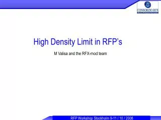
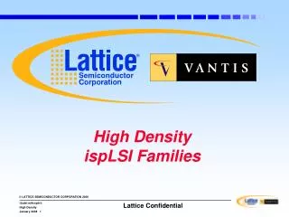
High Density ispLSI Families. High Density. Product Line Expansion. Pins. 400+. 1998 ispLSI 2000E/2000VE 5000V/8000/ispGDX. 300+. 1996. ispLSI 1000E/2000V/3000E/6000. 240. 1994 ispLSI 2000/3000. 120. 1992 ispLSI 1000. 28. 1985 GAL. 0. 0.7K. 8K. 14K. 25K. 50K.

E N D
High Density Product Line Expansion Pins 400+ 1998 ispLSI 2000E/2000VE 5000V/8000/ispGDX 300+ 1996 ispLSI 1000E/2000V/3000E/6000 240 1994 ispLSI 2000/3000 120 1992 ispLSI 1000 28 1985 GAL 0 0.7K 8K 14K 25K 50K Logic Density
ispLSI 1000/E ispLSI Families ispLSI 2000/E & 2000V/VE ispLSI 1000/E ispLSI 3000 ispLSI 6000 ispLSI 3000 ispLSI 5000V ispLSI 8000/V ispLSI 1000/E The Premier High- Density Family - 125MHz/7.5ns Pin-to Pin - 2000 - 8000 PLD Gates - 44-Pin to 128- Pin Pkgs ispLSI 2000/E/V/VE SuperFAST System Performance - 200MHz/3.5ns Pin-to-Pin - 5V/3.3V - 1000 - 6000 PLD Gates - Boundary Scan Test (VE) - 44-Pin to 176-Pin Pkgs ispLSI 3000 High-Density With Performance - 125MHz/7.5ns Pin-to Pin - 7000 - 20,000 PLD Gates - Boundary Scan Test - 160-Pin to 432- Ball Pkgs ispLSI 6000 High-Density With On-Chip Memory - 70MHz/15ns Pin-to Pin - 25,000 PLD Gates - 4K Bit FIFO or RAM - Register/Counter Module - Boundary Scan Test - 208-Pin Pkg ispLSI 5000V SuperWIDE CPLDs - 125MHz/7.5ns Pin-to Pin - 3.3V/2.5V - 12,000 - 24,000 PLD Gates - Boundary Scan Test - 272-Ball to 388- Ball Pkgs ispLSI 8000/V SuperBIG CPLDs - 100MHz/8.5ns Pin-to Pin - 5V/3.3V/2.5V - 25,000 - 50,000 PLD Gates - Boundary Scan Test - 204-Ball to 432- Ball Pkgs
Original ispLSI Families (1K/E, 2K and 3K) Key GAL Features 16V822V1020XV1020RA106002 Prog. Variable XOR Asynch Prod. Term Macrocell Product Clocks Sharing/ Term Input Distribution Registers ispLSI GLB 18XVRA4 NOTE: The 3000 Family Utilizes a 24XVRA8 “Twin GLB” Structure
The 1000/E Family Generic Logic Block Predictable Propagation Delay Can Implement 90% of ALL 4-bit MSI Functions Extremely Flexible and Versatile
1000/E Generic Logic Block: Multi Mode Individual Outputs are Independently Configurable
1000/E Output Routing Pool • Connects GLB Outputs to I/O Cells • Greater Flexibility in Pin Assignment • Improved Routibility • Predictable Delay
1000/E Output Routing Pool Bypass High-Speed Path Faster Tpd & Tco
1000/E Family Clock Network Three Global Clocks To GLBs Two Global Clocks To I/O Cells ispLSI 1016 has 3 Global Clocks
1000/E I/O Cell Configurations • Input, Output and Bi-directional Cells
ispLSI 1048/ 1048C ispLSI 1032 ispLSI 1024 ispLSI 1016 Density (PLD Gates) Speed: Fmax (MHz) Speed: Tpd (ns) Macrocells Registers Inputs & I/Os Pins/Package 2000 111 10 64 96 36 44-PLCC 44-TQFP 44-JLCC 4000 91 12 96 144 54 68-PLCC 100-TQFP 68-JLCC 6000 91 12 128 192 72 84-PLCC 100-TQFP 84-CPGA 8000 80 15 192 288 106/110 120-PQFP 128-PQFP 133-CPGA ispLSI 1000 Family
ispLSI 1000E Family Enhancements • 2nd Generation ispLSI 1000 Product Family • Identical Pin-Out to ispLSI 1000 Family • Except for Addition of Global Output Enable Pins • Provides Much Higher System Performance • ispLSI 1016 Tpd=10ns, Fmax=110 MHz • ispLSI 1016E Tpd=7.5ns, Fmax=125 MHz • Improved I/O Register Speed for Faster Processor Bus Applications • Additional Global OE Pins for Better Tri-State Control and Higher Performance • Enhanced GRP Architecture • More Predictable Delay • Higher Routability • Better Utilization • Add Programmable Output Slew Rate Control to Reduce Ground Bounce and Switch Noise Provides Improvement Over ispLSI 1000 Family!
ispLSI 1032E ispLSI 1000E Family • Lattice’s 2nd Generation 1000 Family • High System Performance • Higher Routability • Higher Utilization ispLSI 1048E ispLSI 1016E Density (PLD Gates) Speed: Fmax (MHz) Speed: Tpd (ns) Macrocells Registers Inputs & I/Os Pins/Package Availability 2000 125 7.5 64 96 36 44-PLCC 44-TQFP NOW 6000 90/125 10/7.5 128 192 72 84-PLCC 100-TQFP NOW 8000 91 10 192 288 110 128-PQFP 128-TQFP NOW
1032 vs. 1032E Comparison Pinout Difference • 1032 and 1032E Identical Except for: • 1032E Adds 2 Global Output Enables • 1032E Has Enhanced Routing Resources • Provides a Performance Migration Path for the 1032
ispLSI 2000 Family Targeted for • Highest Performance • Lowest Cost ispLSI 2000 Family Product Strategy • Supports Most Popular Density and I/O Range • 32 to 128 Macrocells • 32 to 128 I/O • 44 to 176 Pin Packages • Alternative Solution In Terms of Density and I/O Ratio • Twice As Much I/O for a Given Density as Compared to ispLSI 1000/E Family
ispLSI 2000 Family Architecture ispLSI 2064 Block Diagram Global Output Enables Megablock Output Enables GLB With Optimum Input-to-Output Ratio Consistent and Predictable GRP Fast or Slow Slew Rate Flexible Clocking Schemes
ispLSI 2000 Family GLB JK-,T- and D-type flip flops 20 product terms for all four outputs Multiple clocks for synchronous and asynchronous applications 18XVRA4 Product Term Sharing XOR for combinatorial and registered functions
ispLSI 2000 Family ORP • 1:1 ratio of GLB outputs to I/O Cells • Increased routability over the 1000 Family
Architecture Optimized for Performance and Cost ispLSI 2000 Family Summary Architecture Enhancements • Enhanced GRP Architecture • More Predictable GRP Delay • Higher Routability • Better Utilization • Additional Global OEs • Enhanced Tri-State Control • Provide Higher OE Performance • Eliminates I/O Register • Faster Tpd • Eliminates Clock Polarity Option • Faster Tco • Provides Output Slew Rate Control • Reduce Ground Bounce and Switching Noise • Emphasizes TQFP Packaging for ISP Capability
ispLSI 2128 ispLSI 2096 ispLSI 2064 ispLSI 2032 Density (PLD Gates) Speed: Fmax (MHz) Speed: Tpd (ns) Macrocells Registers Inputs & I/Os Pins/Package 1000 180 5.0 32 32 35 44-PLCC 44-TQFP 48-TQFP 2000 125 7.5 64 64 70 84-PLCC 100-TQFP 4000 125 7.5 96 96 104 128-PQFP 128-TQFP 6000 100 10 128 128 138 160-MQFP 176-TQFP ispLSI 2000 Family • Double The I/Os Of 1000 Family • Fastest High-Density PLD Family • New TQFP Options Enhance ISP Capability
2128 2096 1048C/E 2064 I/Os 1032/E 1024 2032 1016/E Macrocells 2000 Family Provides Twice the I/O Compared to 1000/E Family ispLSI 2000 Family Density vs I/O
ispLSI 2000V Family Product Strategy • Lattice First 3.3V High-Density Family • 2000V Family Will Support JTAG Programming Scheme • Targeted to be Fastest 3.3V CPLD in the Market • Strengthens Lattice ISP Position Total ISP ispLSI 2000V is the First 3.3V ISP CPLD Family in the Market!
ispLSI 2000V Family • Industry’s First 3.3V ISP CPLD Family • 2000V Family Supports Open-Drain Outputs • Density Migration Path • Support Mixed 3.3V/5V Systems • JTAG Programming ispLSI 2128V ispLSI 2096V ispLSI 2032LV/ 2032V ispLSI 2064V Density (PLD Gates) Speed: Fmax (MHz) Speed: Tpd (ns) Macrocells Registers Inputs & I/Os Pins/Package 1000 100 7.5 32 32 35 44-PLCC 44-TQFP 2000 100 7.5 64 64 70/37 44-PLCC 44-TQFP 100-TQFP 84-PLCC 4000 80 10 96 96 104 128-PQFP 128-TQFP 6000 80 10 128 128 138/74 176-TQFP 160-PQFP 100-TQFP 84-PLCC
ispLSI 3000 Family Product Strategy • High Density / High Functionality / High Speed • Provides Higher Density and Higher Pin-Count Devices • 160 to 448 Macrocells • 130 to 258 I/O Counts • 160 to 304 Packages • Increased Functionality for Higher System Integration • Achieve Highest Performance • 3192: 10ns (Tpd), 100MHz (Fmax) • Predictable Delay • Boundary Scan Testability Supported Emphasizes Lattice ISP Technology!
ispLSI 3000 Family Architecture 3256 Functional Block Diagram 128 I/Os, 256 Macrocells 384 Registers Global External and Internal Clocks GRP and ORP for Maximum Routing and Utilization In-System Programmable
ispLSI 3000 Family Architecture Enhancements • Highest Density Device • Boundary Scan Testability • Twin GLB Architecture • More Global Clocks • Enhanced GRP Routing Resources • No Fanout Variation In The GRP • Global Output Enables • Programmable Slew Rate
ispLSI 3000 Family ORP • 2:1 ratio of GLB outputs to I/O Cells
ispLSI 3000 Family I/O Cell I/O Cell Functionality the Same as the 1000 Family Test OE to All I/O Cells Global OEs to All I/O Cells
ispLSI 3160 ispLSI 3160 ispLSI 3448 20000 90 12 448 672 226 Yes 432-BGA 2Q98 ispLSI 3000 Family ispLSI 3192 ispLSI 3320 ispLSI 3256E ispLSI 3256A 7000 125 7.5 160 320 162 Yes 208-MQFP 272-BGA* NOW 9000 100 10 192 384 194 Yes 240-MQFP 272-BGA NOW 11000 90 12 256 384 130 Yes 160-MQFP 160-PQFP* NOW 12000 100 10 256 512 258 Yes 304-MQFP 320-BGA NOW 14000 100 10 320 480 162 Yes 208-MQFP 208-PQFP 320-BGA* NOW Density (PLD Gates) Speed: Fmax (MHz) Speed: Tpd (ns) Macrocells Registers Inputs & I/Os Boundary Scan Test Pins/Package Availability * Contact Factory for Availability
Introduction to VantisProgrammable Logic Devices MACH 1 and MACH 2 CPLD FamiliesMACH 5 FamilyMACH 4 FamilyJTAG ISP
Agenda • Vantis value propositions • Vantis MACH 1 CPLD Family • Vantis MACH 2 CPLD Family • Vantis MACH 5 CPLD Family architecture • Vantis MACH 4 CPLD Family architecture • Compare and Contrast • JTAG ISP
Vantis Value Propositions • SpeedLocked performance • Ease-of-Use • Multiple Density - I/O combinations • Reliability • Advanced system integration features
MACH 1 & MACH 2 Architectures Principal performance features of the MACH 1 & MACH 2 Architectures are: • Central switch matrix • Product-Term (PT) arrays -- programmable “AND” planes • Logic Allocators -- fixed “OR” planes • Multimode macrocells • PAL Block OE (Output Enable) Product-Terms
MACH 1 & MACH 2 Features and Characteristics • Original MACH Architectures • Highly Routable • Power Management Feature • Per Macrocell and Per Block power-down • Guaranteed SpeedLocked Timing • up to 12 PT for M1 • up to 16 PT for M2 • Multiple Density and I/O Combinations • Commercial and Industrial Devices Available • Up to sixteen Product-Term functions are accommodated
MACH 1 & MACH 2 Performance: Speeds and Densities • Speed Performance • Commercial as fast as tPD = 5 ns (FCNT = 182 MHz) • Industrial as fast as tPD = 7.5 ns • Mid-Range Densities • 32 to 128 macrocells • 32 to 64 I/Os • 4 to 16 output enable controls
MACH 1 & MACH 2 Performance: System Capabilities • Devices are In-System Programmable (‘SP’ devices only) • Devices are JTAG (IEEE 1149.1) compatible (‘SP’ devices only) • Do not have a boundary-scan register so test is not possible • PCI-compliant (Speed Grades 7 ns, 10 ns and 12 ns • Device I/Os are “Bus-Friendly” • Devices have a programmable security bit • Devices follow a pre-set power-up procedure • Power Management Feature -- Full or Half-Power
MACH 1 & MACH2 Performance: Technology & Support • Leading-edge process technology • The EE6.5 process • L(EFF) = 0.5 micron • Supported by DesignDirect and IDE software • Low-cost entry-level tool • Windows GUI interface
208 Pins 144 100 MACH131SP-5 MACH231SP-10 84 MACH131-7 MACH231-6 MACH120-12 68 MACH221-7 44 Macrocells MACH111(SP)-5(5) MACH215-12 MACH211(SP)-7(7) MACHLV210A-10 256 32 48 64 96 128 MACH 1 & MACH 2 CPLD Families
MACH 1 Block Diagram PAL Block P-T A r r a y (Prog. AND Plane) Logic A l l o c a t o r (Fixed OR Plane) 16 Clock/Input I/O Pins Pins 16 16 16 Output I/O Cells S w i t c h M a t r i x MCs 26 Dedicated Inputs Output Macrocell Feedback I/O Pin Feedback
Fixed OR- Plane MACH 1 P-T Array & Logic Allocator Product-Term Array To Macrocell 4 From Switch Matrix 4 (Max. 12 P-Ts) 4 Programmable AND- Plane
MACH 1 Macrocell PAL-Block Asynchronous Preset 1 From Logic Allocator (4-12 P-Ts) 1 AP 0 To I/O Cell Q D 0 CLK0 AR CLKn PAL-Block Asynchronous Preset To Switch Matrix
P-T A r r a y (Prog. AND Plane) MACH 2 Block Diagram PAL Block Logic A l l o c a t o r (Fixed OR Plane) I/O Pins Clock/Input 8 Pins I/O Cells Output S w i t c h M a t r i x MCs 22/26 8 Buried MCs Buried Macrocell Feedback Output Macrocell Feedback I/O Pin Feedback