Download
1 / 45
480 likes | 605 Vues
Learn efficient communication techniques between hardware accelerators and the processing system (PS) in embedded systems. Topics include AXI interfaces, memory mapping, AXI4 protocol, DMA usage, and custom accelerators for Zynq. Understand the role of GP and HP ports, scatter-gather DMA, AXI master units, and accelerator architecture with DMA. Increase your knowledge on PL-PS interfaces, accelerator communication, and programming sequences for DMA channels in Zynq. Master the techniques for efficient data transfers and processing in embedded systems.

E N D
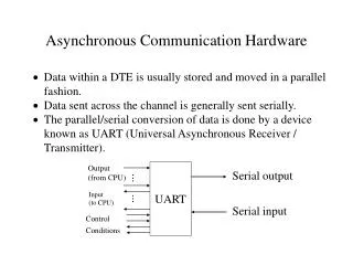
ECE 699: Lecture 8 Efficient Communication Between Hardware Accelerators and PS
Recommended Videos & Slides M.S. Sadri, ZYNQ Training • Lesson 12 – AXI Memory Mapped Interfaces • and Hardware Debugging • Lesson 7 – AXI Stream Interface In Detail (RTL Flow) • Lesson 9 – Software development for ZYNQ using • Xilinx SDK (Transfer data from ZYNQ PL to PS) Xilinx Advanced Embedded System Design on Zynq • Memory Interfacing
Mapping of an Embedded SoC Hardware Architecture to Zynq Source: Xilinx White Paper: Extensible Processing Platform
Simple Custom Peripheral Source: M.S. Sadri, Zynq Training
Simple Custom Accelerator Source: M.S. Sadri, Zynq Training
Example of a Custom Accelerator Source: M.S. Sadri, Zynq Training
Block Diagram of the Pattern Counter Source: M.S. Sadri, Zynq Training
Ways of Implementing AXI4 Slave Units Source: M.S. Sadri, Zynq Training
Pixel Processing Engine Source: M.S. Sadri, Zynq Training
PS-PL Interfaces and Interconnects Source: The Zynq Book
General-Purpose Port Summary • GP ports are designed for maximum flexibility • Allow register access from PS to PL or PL to PS • Good for Synchronization • Prefer ACP or HP port for data transport
High-Performance Port Summary • HP ports are designed for maximum bandwidth access to external memory and OCM • When combined can saturate external memory and OCM bandwidth • – HP Ports : 4 * 64 bits * 150 MHz * 2 = 9.6 GByte/sec • – external DDR: 1 * 32 bits * 1066 MHz * 2 = 4.3 GByte/sec • – OCM : 64 bits * 222 MHz * 2 = 3.5 GByte/sec • Optimized for large burst lengths and many outstanding transactions • Large data buffers to amortize access latency • Efficient upsizing/downsizing for 32 bit accesses
Using Central DMA Source: M.S. Sadri, Zynq Training
Central DMA • High-bandwidth Direct Memory Access (DMA) between a memory-mapped source address and a memory-mapped destination address • Optional Scatter Gather (SG) • Initialization, status, and control registers are accessed through an AXI4-Lite slave interface Source: Xilinx Advanced Embedded System Design on Zynq
Using Central DMA in the Scatter-Gather Mode Source: M.S. Sadri, Zynq Training
Scatter Gather DMA Mode Source: Symbian OS Internals/13. Peripheral Support
Custom Accelerator with the Master AXI4 Interface Source: M.S. Sadri, Zynq Training
Ways of Implementing AXI4 Master Units Source: M.S. Sadri, Zynq Training
AXI4-Full Source: M.S. Sadri, Zynq Training
Image Rotation Unit Source: M.S. Sadri, Zynq Training
FFT Unit Source: M.S. Sadri, Zynq Training
Sample Generator Source: M.S. Sadri, Zynq Training
PL-PS Interfaces Source: M.S. Sadri, Zynq Training
Accelerator Architecture with DMA Source: Building Zynq Accelerators with Vivado HLS, FPL 2013 Tutorial
AXI DMA-based Accelerator Communication • Write to Accelerator • processor allocates buffer • processor writes data into buffer • processor flushes cache for buffer • processor initiates DMA transfer • Read from Accelerator • processor allocates buffer • processor initiates DMA transfer • processor waits for DMA to complete • processor invalidates cache for buffer • processor reads data from buffer
Flushing and Invalidating Cache /* Flush the SrcBuffer before the DMA transfer */ Xil_DCacheFlushRange((u32)TxBufferPtr, BYTES_TO_SEND); . . . . . . . . /* Invalidate the DstBuffer after the DMA transfer */ Xil_DCacheInvalidateRange((u32)RxBufferPtr, BYTES_TO_RCV);
Simple DMA Transfer Programming Sequence for MM2S channel (1) Start the MM2S channel running by setting the run/stop bit to 1, MM2S_DMACR.RS = 1. If desired, enable interrupts by writing a 1 to MM2S_DMACR.IOC_IrqEn and MM2S_DMACR.Err_IrqEn. Write a valid source address to the MM2S_SA register. Write the number of bytes to transfer in the MM2S_LENGTH register. The MM2S_LENGTH register must be written last. All other MM2S registers can be written in any order.
Simple DMA Transfer Programming Sequence for S2MM channel (1) Start the S2MM channel running by setting the run/stop bit to 1, S2MM_DMACR.RS = 1. If desired, enable interrupts by by writing a 1 to S2MM_DMACR.IOC_IrqEn and S2MM_DMACR.Err_IrqEn. Write a valid destination address to the S2MM_DA register. Write the length in bytes of the receive buffer in the S2MM_LENGTH register. The S2MM_LENGTH register must be written last. All other S2MM registers can be written in any order.
Transmitting and Receiving a Packet Using High-Level Functions /* Transmit a packet */ Status = XAxiDma_SimpleTransfer(&AxiDma,(u32) TxBufferPtr, BYTES_TO_SEND, XAXIDMA_DMA_TO_DEVICE); if (Status != XST_SUCCESS) { return XST_FAILURE; } while (!TxDone); . . . . . . /* Receive a packet */ Status = XAxiDma_SimpleTransfer(&AxiDma,(u32) RxBufferPtr,BYTES_TO_RCV, XAXIDMA_DEVICE_TO_DMA); if (Status != XST_SUCCESS) { return XST_FAILURE; } while (!RxDone);
Transmitting a Packet Using Lower-Level Functions /* Transmit a packet */ Xil_Out32(AxiDma.TxBdRing.ChanBase + XAXIDMA_SRCADDR_OFFSET, (u32) TxBufferPtr); Xil_Out32(AxiDma.TxBdRing.ChanBase + XAXIDMA_CR_OFFSET, Xil_In32(AxiDma.TxBdRing.ChanBase +XAXIDMA_CR_OFFSET) | XAXIDMA_CR_RUNSTOP_MASK); Xil_Out32(AxiDma.TxBdRing.ChanBase + XAXIDMA_BUFFLEN_OFFSET, BYTES_TO_SEND); while (TxDone == 0);
Receiving a Packet Using Lower-Level Functions /* Receive a packet */ Xil_Out32(AxiDma.RxBdRing.ChanBase + XAXIDMA_DESTADDR_OFFSET, (u32) RxBufferPtr); Xil_Out32(AxiDma.RxBdRing.ChanBase+XAXIDMA_CR_OFFSET, Xil_In32(AxiDma.RxBdRing.ChanBase+XAXIDMA_CR_OFFSET) | XAXIDMA_CR_RUNSTOP_MASK); Xil_Out32(AxiDma.RxBdRing.ChanBase + XAXIDMA_BUFFLEN_OFFSET, BYTES_TO_RCV); while (RxDone == 0);
PL-PS Interfaces Source: M.S. Sadri, Zynq Training
Accelerator Architecture with Coherent DMA Source: Building Zynq Accelerators with Vivado HLS, FPL 2013 Tutorial
Coherent AXI DMA-based Accelerator Communication • Write to Accelerator • processor allocates buffer • processor writes data into buffer • processor flushes cache for buffer • processor initiates DMA transfer • Read from Accelerator • processor allocates buffer • processor initiates DMA transfer • processor waits for DMA to complete • processor invalidates cache for buffer • processor reads data from buffer
Accelerator Coherency Port (ACP) Summary • ACP allows limited support for Hardware Coherency • – Allows a PL accelerator to access cache of the Cortex-A9 processors • – PL has access through the same path as CPUs including caches, OCM, DDR, and peripherals • – Access is low latency (assuming data is in processor cache) no switches in path • ACP does not allow full coherency • – PL is not notified of changes in processor caches • – Use write to PL register for synchronization • ACP is compromise between bandwidth and latency • – Optimized for cache line length transfers • – Low latency for L1/L2 hits • – Minimal buffering to hide external memory latency • – One shared 64 bit interface, limit of 8 masters
AXI-based DMA Services • Four AXI-based DMA services are provided • Central DMA (CDMA) • Memory-to-memory operations • DMA • Memory to/from AXI stream peripherals • FIFO Memory Mapped To Streaming • Streaming AXI interface alternative to traditional DMA • Video DMA • Optimized for streaming video application to/from memory Source: Xilinx Advanced Embedded System Design on Zynq
Streaming FIFO Source: Xilinx Advanced Embedded System Design on Zynq
Streaming FIFO • General AXI interconnect has no support for the AXI stream interface • axi_fifo_mm_s provides this facility • FIFO included • Added as all other types of IP are from the IP Catalog • Features • AXI4/AXI4-Lite slave interface • Independent internal 512B-128KB TX and RX data FIFOs • Full duplex operation Source: Xilinx Advanced Embedded System Design on Zynq
Streaming FIFO • Slave AXI connection • RX/TX FIFOs • Interrupt controller • Control registers • Three user-side AXI Stream interfaces • TX data • RX data • TX control
Energy and Performance Exploration of Accelerator Coherency Port Using Xilinx ZYNQ Mohammadsadegh Sadri, Christian Weis, Norbert When and Luca Benini Department of Electrical, Electronic and Information Engineering (DEI) University of Bologna, Italy Microelectronic Systems Design Research Group, University of Kaiserslautern, Germany {mohammadsadegh.sadr2,luca.benini}@unibo.it, {weis,wehn}@eit.uni-kl.de ver0
Processing Task Definition • We define : Different methodsto accomplish the task. • Measure : Execution time & Energy. Allocated by: kmalloc dma_alloc_coherent Depends on the memory Sharing method Source Image (image_size bytes) @Source Address Selection of Pakcets: (Addressing) - Normal - Bit-reversed Result Image (image_size bytes) @Dest Address 128K Loop: N times Measure execution interval. Image Sizes: 4KBytes 16K 65K 128K 256K 1MBytes 2MBytes FIFO: 128K FIR read write process 41
Memory Sharing Methods • ACP Only (HP only is similar, there is no SCU and L2) Accelerator SCU L2 DRAM ACP • CPU only (with&without cache) CPU 2 • CPU ACP • (CPU HP similar) 1 Accelerator SCU L2 DRAM ACP ACP --- CPU --- ACP --- 42
Speed Comparison ACP Loses! CPU OCM between CPU ACP & CPU HP 298MBytes/s 239MBytes/s 4K 16K 1MBytes 64K 128K 256K 43
Energy Comparison CPU only methods : worst case! CPU OCM always between CPU ACP and CPU HP CPU ACP ; always better energy than CPU HP0 When the image size grows CPU ACP converges CPU HP0 44
Lessons Learned & Conclusion • If a specific task should be done by accelerator only: • For small arrays ACP Only & OCM Only can be used • For large arrays (>size of L2$) HP Only always acts • better. • If a specific task should be done by the • cooperation of CPU and accelerator: • CPU ACP and CPU OCM are always • better than CPU HP in terms of energy • If we are running other applications which • heavily depend on caches, CPU OCM and then • CPU HP are preferred! 45