Download
1 / 19
200 likes | 462 Vues
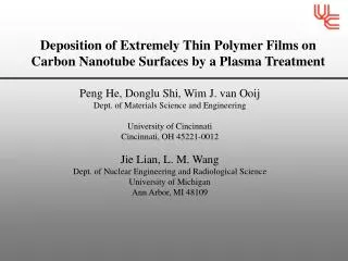
Deposition of Extremely Thin Polymer Films on Carbon Nanotube Surfaces by a Plasma Treatment. Peng He, Donglu Shi , Wim J. van Ooij Dept. of Materials Science and Engineering University of Cincinnati Cincinnati, OH 45221-0012 Jie Lian , L. M. Wang

E N D
Deposition of Extremely Thin Polymer Films on Carbon Nanotube Surfaces by a Plasma Treatment Peng He, Donglu Shi, Wim J. van Ooij Dept. of Materials Science and Engineering University of Cincinnati Cincinnati, OH 45221-0012 Jie Lian, L. M. Wang Dept. of Nuclear Engineering and Radiological Science University of Michigan Ann Arbor, MI 48109
What are Carbon Nanotubes? Carbon nanotube is a new carbon allotrope that was first discovered in 1991 by Dr. Sumio Iijima at NEC. It has a nanometer-scale hollow tubular structure and a different atomic arrangement from graphite, diamond and C60 bucky-ball C the other three known carbon structures. Its unique and promising properties have attracted the attention of researcher around the world and led to active R&D efforts in the commercial industries.
Properties of Carbon nanotubes • the highest elastic module, and mechanical strength that is approximately 200 times stronger than steel. • novel electronic properties. • high thermal conductivity. • excellent chemical and thermal stability. • promising electron field emission properties. • high chemical (such as lithium) storage capacity.
SWNT and MWNT Single-Wall Nanotube (SWNT) Multi-Wall Nanotube (MWNT) TEM Image of MWCNT
Synthesis Method of CNT I. Arc Discharge Method Without Catalyst → MWNT With Catalyst (Co, Ni, Fe, etc.) → SWNT
Synthesis Method of CNT II. Laser Ablation Method Without Catalyst →Fullerene With Catalyst (Co, Ni, Fe, etc.) → SWNT
Synthesis Method of CNT III. Chemical Vapor Deposition (CVD) MWCNT 600-800 ° C2H2→ 2C + H2 SWCNT 900-1000 ° 2CO → C + CO2
Applications of Carbon Nanotubes • telecommunication, cell phones. • rechargeable lithium batteries. • medical image equipment. • computer display. • multi-functional composites for aircraft.
Applications of Carbon Nanotubes Carbon Nanotube FED Panel Carbon Nanotube computer
Plasma Process Parameters: • Basic pressure: < 40 mTorr • Monomer used: C6F14 • Monomer pressure: 200 ~ 250 mTorr • System total pressure: < 300 mTorr • RF frequency: 13.56 MHz • Input power: 5-30 Watt • Treatment time: 5-30 minutes • Per batch: 0.2-1 grams
HRTEM of coated MWNT (B) (A) 200 nm 200 nm
(A) (B) inner coating 1~3 nm Outer surface 0.34 nm Outer coating ~7 nm 5 nm 10 nm HRTEM of coated MWNT
(A) (B) Outer Coating ~5 nm Outer coating ~2 nm 20 nm 10 nm HRTEM of coated MWNT
positive negative O– C2 C2 C1 C3 OH– C1 Cl– Br– C4H– C4– C4 C5 C6 C7H7+ C6H4-C2H3O2+ C10H8+ C7H8Cl– C6H4-C4H5O2+ C11H14Cl– TOFSIMS of untreated Nanotubes
positive negative CF+ C+ C2H5+ F– H+ C2H3+ F2– C2F+ CF3+ CF3– C2F– C2F4+ C3F3+ C3F3– C2F5+ C2F5– C5F3– C3F5+ C3F5– C5F5– C7F3– C4F5– C4F7+ C3F7+ C3F7– C4F6+ C4F7– C5F7– C5F7+ TOFSIMS of C6F14- plasma-treated nanotubes
HRTEM of coated SWNT Coated SWNT bundles SWNT bundles Polymer Coating 10 nm
HRTEM of coated SWNT Coated SWNT 2.1 nm 10 nm
HRTEM of coated SWNT Wall diameter ~1.4 nm Polymer Coating 10 nm
Conclusion • An ultrathin film of polymer deposited on the surfaces of MWNT by means of a plasma polymerization treatment. • The polymer layer is not only uniform on outer surfaces, but also deposited in an extremely thin thickness of 2~7 nm. • This unique plasma coating opens great possibilities for future novel engineering applications.