Welcome to Solid State Devices !
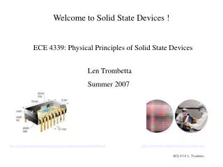
Welcome to Solid State Devices !. ECE 4339: Physical Principles of Solid State Devices. Len Trombetta Summer 2007. http://www.intel.com/technology/silicon/index.htm. http://www.tiscali.co.uk/reference/encyclopaedia/hutchinson/m0030289.html. Proper Terminology.

Welcome to Solid State Devices !
E N D
Presentation Transcript
Welcome to Solid State Devices ! ECE 4339: Physical Principles of Solid State Devices Len Trombetta Summer 2007 http://www.intel.com/technology/silicon/index.htm http://www.tiscali.co.uk/reference/encyclopaedia/hutchinson/m0030289.html ECE 4339 L. Trombetta
Proper Terminology Solid State: (1) A branch of physics dealing with solids (as opposed to liquids or gases). (2) A reference to electronic devices made using semiconductors (e.g., BJTs, diodes, FETs…). Incorrect terminology: “solid states” Semiconductor: A class of materials used in the manufacture of solid state devices. Incorrect usage: “The heart of the computer is Intel’s new 3.6 GHz semiconductor.” (Semiconductor should be replaced by Microprocessor, or perhaps Integrated Circuit.) ECE 4339 L. Trombetta
Terminology… Silicon (Si): (sill i con) A column IV element that is a semiconductor at room temperature. It is widely used in the manufacture of integrated circuits, especially consumer electronics. From Webelements.com Silicone: (sill i cone) A rubbery material used as a sealant or to patch leaks. From Specialty Silicone Products Inc. web site ECE 4339 L. Trombetta
Structure Overview Electromagnetic (mostly statics) Quantum Physics (not much in this course) Crystallography Semiconductor Physics electrical and optical properties Schottky diode (metal-semiconductor junction) p-n junction diode BJT and variations: HBT FET: JFET, MOSFET (CMOS) LED/Laser Diode ECE 4339 L. Trombetta
Gate Source In state-of-the-art FETs, this layer will be less than 20 Å thick. Drain Metal-Oxide-Semiconductor Field-Effect-Transistor An “MOS” device (a MOSFET). If we remove the source and drain, we have a simpler device: the MOS capacitor (MOSC). The MOSC has numerous applications itself; arrays of MOSC’s are the sensing elements in a CCD digital camera. Operation: If the voltage at the gate is larger than the threshold (VT), and the drain is positive w/r the source, a current will flow below the oxide from drain to source. ECE 4339 L. Trombetta
Moore’s Law… Moore’s Law… This .pdf is from Intel’s web site. It is available on Blackboard under “Course Documents”. ECE 4339 L. Trombetta
Common Semiconductor Applications • Group IV • Si for MOS, particularly CMOS digital logic and memory • Si BJT for some logic and analog applications • SiC for high power, high temperature applications • Ge for diodes, BJTs • Group III/V • GaAs, GaAsP, InP for optoelectronic and high speed digital applications • InAs/GaInSb/AlInSb for long wavelength detectors • GaN, AlGaN for blue/white LEDs and high power devices • Group II/VI • CdTe, HgCdTe for long wavelength detectors Pronunciation: Generally, we can simply recite the name of each element, truncate the last one, and add “ide” to the end. For example, InGaAsP is “indium gallium arsenic phosphide”. ECE 4339 L. Trombetta
ECE 4339 L. Trombetta Reference: www.dayah.com/periodic/
Semiconductor Properties This is a page from the notes on the web. It will come in handy for calculations and quizzes/exams and homework. ECE 4339 L. Trombetta
Materials used to fabricate integrated circuits include some from all three classifications. Amorphous: insulators (SiO2) Polycrystalline: MOS gates; contacts Crystalline: substrates ECE 4339 L. Trombetta
The entire crystal can be “generated” by suitable placement of (infinitely) many unit cells. The unit cell is not unique: here are two examples (b) and (d). ECE 4339 L. Trombetta
a b c The lattice can be “constructed” by moving the unit cell along the lattice vectors where p, q, and s are integers. The figures here are all unit cells that can be used to construct the lattice. For bcc and fcc there are simpler unit cells, called “primitive cells” (not shown) that can also be used. However, they are harder to visualize. ECE 4339 L. Trombetta
The Bravais lattices are mathematical constructions: they represent all the ways that points can be arranged in 3-D space so that all the points have exactly the same surroundings. Reference: Pierret, Modular Series on Solid State Devices vol. VI, Addison-Wesley ECE 4339 L. Trombetta
The diamond lattice can be thought of as two inter-penetrating fcc lattices. The dark blue and green dots represent one fcc lattice. The light blue represent another fcc lattice that has been translated to the point indicated by the red vector. http://phycomp.technion.ac.il/~nika/diamond_structure.html ECE 4339 L. Trombetta
Another way to think of the diamond lattice is this: Imagine that the fcc lattice (top figure) has attached to it, at the bottom right corner, the two atoms indicated in red below. If we attach these two atoms to each of the fcc lattice sites, the result is the diamond lattice. (We call this “lattice with a basis”, where the basis is the two red atoms.) ECE 4339 L. Trombetta
Diamond cutters know how to make diamonds split along certain planes. Photos from The Diamond Guy: Diamond Education http://www.diamondcuttersintl.com/diamond_education/photogallery/shapes/shapes.html ECE 4339 L. Trombetta
Photo from Wacker Siltronics website: http://www.siltronic.com/int/noc ECE 4339 L. Trombetta
We can add a single atomic layer at a time to a substrate using various “epitaxial” techniques. Epitaxial Growth Molecular Beam Epitaxy System in the William R. Wiley Environmental Molecular Sciences Laboratory is used to grow and characterize thin crystalline films of oxides and ceramics to understand in detail the chemistry that occurs on oxides and ceramic surfaces Source: Wikipedia http://en.wikipedia.org/wiki/Molecular_beam_epitaxy ECE 4339 L. Trombetta
For 5 points (out of 100) on Quiz 1: Q1: Give one example each for the primitive unit cells of the fcc and bcc lattices. Q2: What is the structure of the superconductor YBCO? Be prepared to give a brief (~ 3 min) presentation on your answer to the question. You are encouraged to have one or two Power Point slides. Bonus Questions ECE 4339 L. Trombetta

