Some Microwave Devices
Some Microwave Devices. Impatt Diodes PIN Diodes Varactor Diodes YIG Devices (Yttrium-Iron Garnet) Dielectric Resonators BIPOLAR TRANSISTORS GaAsFETs HEMT – High Electron Mobility Transistors. Microwave Solid State Devices.

Some Microwave Devices
E N D
Presentation Transcript
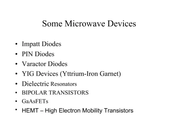
Some Microwave Devices • Impatt Diodes • PIN Diodes • Varactor Diodes • YIG Devices (Yttrium-Iron Garnet) • Dielectric Resonators • BIPOLAR TRANSISTORS • GaAsFETs • HEMT – High Electron Mobility Transistors
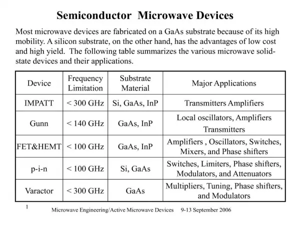
Microwave Solid State Devices • Two problems with conventional transistors at higher frequencies are: 1. Stray capacitance and inductance. - remedy is interdigital design. 2.Transit time. - free electrons move quicker than holes therefore change from silicon to Gallium Arsenide
Microwave Transistors • Conventional bipolar transistors are not suitable for microwave frequencies. • Electrons move faster than holes. • Component leads introduce elevated reactance. • XL increases and XC decreases therefore collector feedback becomes worse as frequency increases. • Transit time and mobility of carriers. As transit time approaches signal period phase shifts occur.
Microwave Transistors • REMEDIES: • Interdigital design of emitter and base minimizes capacitances. • Gallium arsenide. Faster than silicon. • N type GaAsFET. Why N type? • Flat component leads.
Microwave Transistors • REMEDIES contd.: • Low noise design considerations: * Planar and epitaxial methods of construction use diffusion and surface passivation to protect surfaces from contamination as opposed to diffusion method of mesa structure implementing acid etching. * Shot noise is proportional to the square of current therefore operate at moderate Ic. * Thermal noise is reduced at lower power levels. With interdigital base design Rb is low therefore lower voltage drop and less power.
Gunn Devices • Uses phase shift to minimize transmit time. • Transferred-electron device (TED). • N type GaAs – electron mobility decreases as electric field strength increases. • Characterized by a negative resistance region. • A domain is developed that sustains oscillations as a voltage is applied to the substrate of GaAS. • A pulse current develops as domain of charge travels to the positive terminal.
Other Devices • Pin Diodes - R.B.(R II C) F.B. (variable R) • Varactor Diodes – R.B. (variable junction capacitance) • YIG Yitrium-Iron-Garnet Devices • Dielectric Resonators • MMICs – monolithic microwave integrated circuits
HEMT • High Electron Mobility Transistor • Similar to GaAsFET construction. • Difference is that motion of charge carriers is confined to a thin sheet within a GaAs buffer layer. • GaAs/AlGaAs heterostructure epitaxy. • The thickness of the channel remains constant while the number of carriers is modulated by the gate bias as opposed to a MESFET that modulates the channel thickness. • PHEMT- pseudomorphic HEMT used above 20 GHz (mm wave)
Microwave Tubes • Magnetrons • Klystrons • Travelling-Wave Tube
Microwave Horn Antennas E-plane H-plane Pyramidal Conical Slot


