Understanding 3D Die Maps: Definition, Profiles, and Analysis Techniques
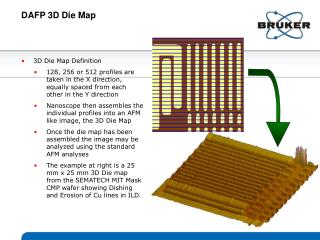
The 3D Die Map is a crucial tool in semiconductor fabrication, representing an AFM-like image constructed from either 128, 256, or 512 profiles taken in the X direction and spaced evenly in the Y direction. The Nanoscope software assembles these profiles into a comprehensive image for detailed analysis. This method allows for the inspection of critical features such as dishing and erosion in Cu lines within inter-layer dielectrics. An example map, measuring 25 mm x 25 mm, illustrates these phenomena on a SEMATECH MIT Mask CMP wafer.

Understanding 3D Die Maps: Definition, Profiles, and Analysis Techniques
E N D
Presentation Transcript
DAFP 3D Die Map • 3D Die Map Definition • 128, 256 or 512 profiles are taken in the X direction, equally spaced from each other in the Y direction • Nanoscope then assembles the individual profiles into an AFM like image, the 3D Die Map • Once the die map has been assembled the image may be analyzed using the standard AFM analyses • The example at right is a 25 mm x 25 mm 3D Die map from the SEMATECH MIT Mask CMP wafer showing Dishing and Erosion of Cu lines in ILD.