Progress on resistive anodes and the large Prototype TPC
170 likes | 202 Vues
Explore the necessity of resistive films, recent resolution breakthroughs, R&D goals for the large prototype, bulk technologies, and work with the After chip in EUDET and T2K. Learn about photovoltaic techniques and simulation work predicting properties for robust resistive anodes. Discover how modifying Micromegas with resistive films can improve resolution limitations in traditional TPCs and achieve the ILC resolution goal. Follow progress in developing large prototype panels and resistive functionality using the AFTER electronics technology with SiPM. Explore options for resistive anodes and the potential of photovoltaic technologies for cost-effective large surface applications. Simulation work continues to redefine resistive pastes and films for improved results.

Progress on resistive anodes and the large Prototype TPC
E N D
Presentation Transcript
Progress on resistive anodes and the large Prototype TPC By: Stephen Turnbull
Outline • Why resistive films are necessary • Resolution records broken just this last year • A brief look at R&D Goals for the large prototype • Bulk technologies • Further work with the After chip developed for EUDET and used in T2K • Learning about photovoltaic techniques • Simulation work to predict desired properties • Next steps robustes,
Traditional spatial resolution limits • Traditional TPCs are limited in resolution by the Cluster width/pad width ratio. In short, only clusters E and F can be told apart from A,B,C,and D. • So with traditional TPC’s the options to improve resolution are • A. Increase Cluster sizes; • high Transverse diffusion gas • GEM stacks • Post amplification gas volume • B. or Decrease Pad Width; more channels.
Charge dispersion in a MPGD with a resistive anode • 2D Telegraph equation: • Modified MPGD anode with a high resistivity film bonded to a readout plane with an insulating spacer • Point charge at r = 0 & t = 0 disperses with time • The charge density r(r,t) at (r,t) is a solution of the 2D Telegraph equation • The anode charge density is time dependent and sampled by readout pads Q(t) (r) mesh resistive foil glue pads (r,t) integral over pads PCB M.S.Dixit et.al., NIM A518 (2004) 721 r (mm) t (ns)
Extrapolation of the ILC TPC Left: Micromegas with high Transverse diffusion gas( Analytical model). Best possible resolution in a very narrow window (150 – 350 mm) for 1mm pitch pads.Right, Black: Micromegas with Low diffusion gas, standard thin pads would be limited to a minimum of 130 resolution. Right Red: Micromegas with a resistive film and wide, 2.3 mm, pads. The ILC resolution goal can be achieved.
The Carleton chamber Carleton-Saclay Micromegas endplate with resistive anode. 128 pads (126 2mmx6mm in 7 rows plus 2 large trigger pads) Drift length: 15.7 cm ALEPH preamps + 200 MHz digitizers
The 5T cosmic-ray test at DESY 4 weeks of data taking (thanks to DESY and T. Behnke et al.) Used 2 gas mixtures: Ar+5% isobutane (easy gas, for reference) Ar+3% CF4+2% isobutane (so-called T2K gas, good trade-off for safety, velocity, large wt ) Most data taken at 5 T (highest field) and 0.5 T (low enough field to check the effect of diffusion) Note: same foil used since more than a year. Still works perfectly. Was ~2 weeks at T=55°C in the magnet: no damage
Resolution = 50 µ independent of the drift distance ‘T2K gas’ Resolution of 1/40th of pad width achieved! Results from these tests now published http://dx.doi.org/10.1016/j.nima.2007.07.099
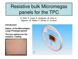
Our Next big goal Large Prototype panels f = 80cm Panels to be ready by the end of 2007, Cosmic tests to commence in January 2008 Beam tests starting summer 2008. All using AFTER Electronics Technology: Resistive Bulk Trigger : SiPM
Now add Resistive Functionality • Carleton-CERN-Orsay-Saclay… + others R&D collaboration towards a resistive ‘bulk’ Micromegas. • Options for the resistive anode: • Resistive paste (under test at CERN) • Resistive film (AlSi cermet) on mylar+glue • Thin film deposition on PCB or kapton or other (project at Neuchatel)
SCA: 76x511 Cells Front-end ASIC “AFTER” Technology: AMS CMOS 0.35mm Number of transistors: 400,000 Area: 7546mm x 7139 mm Package: LQFP 160 pins; 30 x 30 x 1.4 mm pitch: 0.65 mm Submission: 24 April 2006 Delivery: end of July 2006 Characterization: October 2006 – March 2007 Design features • 72 channels x 511 analog memory cells; Fwrite: 1-50 MHz; Fread: 20 MHz • 4 Charge Ranges (120 fC; 240 fC; 360 fC & 600 fC) • 16 Peaking Time Values (100 ns to 2 µs) – Or no shaping if desired. • MIP/noise: 100; I.N.L: 1% [0;3 Mips], 5% [3-10 Mips]
What we hope to do with Photovoltaic technologies • Deposits of resistive layers • Deposits of thin metal conductive pads • Learning about connections • LARGE surfaces at low Low LOW costs.
Simulation work yet still to come • Defining the relationship between the PRF and ultimate resolution. • Defining a new model for resistive pastes, rather then restive films sitting on a non-conducting glue
People I’ve stolen slides from • P. Colas • M. Dixit via D.Attie • D.Attie • M. Riallot (DAPNIA/SEDI) • D. P. Peterson • D. Calvet • And myself of course
