Download
1 / 25
580 likes | 1.28k Vues
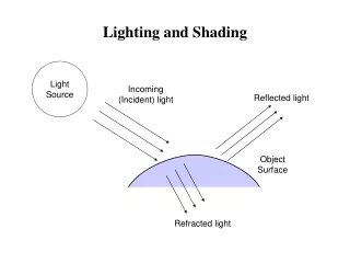
Chapter 5 Lithography. Introduction and application. Light source and photomask, alignment. Photolithography systems. Resolution, depth of focus, modulation transfer function. Other lithography issues: none-flat wafer, standing wave... Photoresist.

E N D
Chapter 5 Lithography Introduction and application. Light source and photomask, alignment. Photolithography systems. Resolution, depth of focus, modulation transfer function. Other lithography issues: none-flat wafer, standing wave... Photoresist. Resist sensitivity, contrast and gray-scale photolithography. Step-by-step process of photolithography. NE 343: Microfabrication and thin film technology Instructor: Bo Cui, ECE, University of Waterloo; http://ece.uwaterloo.ca/~bcui/ Textbook: Silicon VLSI Technology by Plummer, Deal and Griffin
Three basic methods of wafer exposure Less mask wear /contamination, less resolution (depend on gap). High resolution. But mask wear, defect generation. No mask wear/contamination, mask de-magnified 4 (resist features 4 smaller than mask). Very expensive, mainly used for IC industry. Fast, simple and inexpensive, choice for R&D.
Near field/Fresnel diffraction for contact/proximity exposure Figure 5.14 Near field: (g is gap) (t is resist thickness) For g=10m, =365nm Wmin 2 m • Interference effects and diffraction result in “ringing” and spreading outside the aperture. • Edges of image rise gradually (not abrupt) from zero. • Intensity of image oscillates about the expected intensity. • Oscillations decay as one approaches the center of the image. • The oscillations are due to constructive and destructive interference of Huygen’s wavelets from the aperture in the mask. • When aperture width is small, the oscillations are large • When aperture width is large, the oscillations rapidly die out, and one approaches simple ray tracing when aperture >> .
Far field/Fraunhofer diffraction for projection exposure Near field Far field Figure 5.15 Far field: W2 << (g2+r2)1/2, r is position on the wafer. Sharp maximum intensity at x=0, and intensity goes through 0 at integer multiples of one-half number.
Quartz UV Mask Diffraction patterns Chrome 4 4 3 3 2 2 1 1 0 Lens Lens capturing diffracted light Large lens captures more diffracted light, and those higher order diffracted light carries high frequency (detail of fine features on mask) information.
Numerical aperture of a lens Numerical aperture (NA) of an optical system is a measure of the ability of the lens to collect light. NA nsin, n is refractive index for the medium at the resist surface (air, oil, water). For air, refractive index n=1, NA = sin (d/2)/f d for small .
Pinhole masks Lens NA Image results (not in same scale) Bad Exposure light Poor Good Diffracted light Effect of numerical aperture on imaging Small lens Large lens
Light diffraction through a small circular aperture Figure 5.6 Qualitative example of a small aperture being imaged. “Airy disk” Light intensity on image plate Figure 5.7 Image intensity of a circular aperture in the image plane. A point image is formed only if 0, f 0 or d. http://en.wikipedia.org/wiki/Airy_disk
Rayleigh criteria for resolution Lord Rayleigh Figure 5.8 Rayleigh suggested that a reasonable criterion for resolution is that the central maximum of each point source lie at the first minimum of the Airy pattern. Strictly speaking, this and next slides make sense only for infinitely far (>>f) objects, like eye. Fortunately, 4x reduction means far object, and near (near focal plane) image. Resolved images Unresolved images
Rayleigh criteria for resolution R S1 S2 S1 S2 S1 S2 K1 factor has no well-defined physical meaning. It is an experimental parameter, depends on the lithography system and resist properties. To increase resolution, one can: Increase NA by using large lens and/or immersion in a liquid (n>1). Decrease k1 factor (many tricks to do so). Decrease (not easy, industry still insists on 193nm).
Effect of imaging/printing conditions Annular means an “off-axis illumination” method, which is one trick to decrease k1. EUV: extreme UV, here wavelength 13.5nm. Immersion means exposure in water.
Depth of focus (DOF) DOF for photography DOF is the range in which the image is in focus and clearly resolved. Large DOF A small aperture was used to ensure the foreground stones were as sharp as the ones in the distance. Small DOF (background blurred) DOF Focal point What one need here is a telephoto lens at its widest aperture.
Rayleigh criteria for depth of focus (DOF) Rayleigh criteria: the length of two optical paths, one on-axis, one from lens edge or limiting aperture, not differ by more than /4. For small B D C O A Again, like the case of resolution, we used k2 factor as an experimental parameter. It has no well-defined physical meaning. Figure 5.9 On axis, optical path increased by OC-OB=. From edge, increased by AC-AB=DC=cos. At point B (focal point), two branches have equal path.
Depth of focus for projection photolithography • It can be seen that larger NA gives smaller depth of focus! • This is also true for camera. A cheap camera takes photos that are always in focus no matter where the subject is, this is because it has small lenses. • This of course works against resolution where larger NA improves this property. • In order to improve resolution without impacting DOF too much, λ has been reduced and “optical tricks” have been employed. Large lens (large NA), small DOF Small lens (small NA), large DOF
Optimal focal plane in photolithography • Light should be focused on the middle point of the resist layer. • In IC, DOF is << 1m, hard to focus if wafer is not super flat. • People talks more of resolution, but actually DOF can often be a bigger problem than resolution. • For example, a 248nm (KrF) exposure system with a NA = 0.6 would have a resolution of 0.3μm (k1 = 0.75) and a DOF of only ±0.35μm (k2 = 0.5). Focal plane Depth of focus
Modulation transfer function (MTF) Modulation transfer function is another useful concept. It is a measure of image contrast on resist. Figure 5.10
MTF and spatial coherence Usually MTF > 0.5 is preferred. It depends on , light source size (coherency), and optical system. It certainly also depends on feature size (or period for a grating pattern). Spatial coherence of light source Point source is coherent • Coherent light will have a phase to space relationship. • Incoherent light or light with only partial coherence will have wave-fronts that are only partially correlated. • Spatial coherence S is an indication of the angular range of light waves incident on mask, or degree to which light from source are in phase. • Small S is not always good (see next slide). Plane wave Partially coherent Figure 5.12
MTF and spatial coherence 2W MTF vs. diffraction grating period on mask. W = line width = space width of the grating. X-axis of the plot: spatial frequency =1/(2W), normalized to Rayleigh criterion cutoff frequency 0=1/R=NA/(0.61). Grating photomask For a source with perfect spatial coherence S=0, MTF drops abruptly at Rayleigh criterion W=half pitch=R=k1/NA. Large S is good for smaller features, but bad for larger ones. Trade-off is made, and industry chooses S=0.5-0.7 as optimal. Large features Smaller features (similar to Figure 5.13)
Chapter 5 Lithography Introduction and application. Light source and photomask, alignment. Photolithography systems. Resolution, depth of focus, modulation transfer function. Other lithography issues: none-flat wafer, standing wave... Photoresist. Resist sensitivity, contrast and gray-scale photolithography. Step-by-step process of photolithography. NE 343 Microfabrication and thin film technology Instructor: Bo Cui, ECE, University of Waterloo Textbook: Silicon VLSI Technology by Plummer, Deal and Griffin
Exposure on patterned none-flat surface This leads to random reflection/proximity scattering, and over or under-exposure. Proximity scattering Both problems would disappear if there is no reflection from substrate.
Exposure on patterned none-flat surface • To reduce the problem, one can: • Use absorption dyes in photoresist, thus little light reaches substrate for reflection. • Use anti-reflection coating (ARC) below resist. • Use multi-layer resist process (see figure below) • thin planar layer for high-resolution imaging (imaging layer). • thin develop-stop layer, used for pattern transfer to 3 (etch stop). • thick layer of hardened resist (planarization layer).
Surface reflection and standing wave • Resist is partially reflective, so some light reaches resist bottom and is reflected. • Constructive and destructive interference between incident and reflected light results in a periodic intensity distribution across the resist thickness. • With change in exposure (light intensity) comes change in resist dissolution rate, leading to zigzag resist profile after development. • Use of anti-reflecting coating (ARC) eliminates such standing wave patterns. • Post exposure bake also helps by smoothing out the zigzag due to resist thermal reflow. • (Also due to reflection, a metal layer on the surface will require a shorter exposure than exposure over less reflective film.) Figure 5.24
Standing wave effect on photoresist /2nPR Photoresist Substrate nPR is refractive index of photoresist Overexposure Underexposure Is this a positive or negative resist?
Position of minimum and maximum intensity Maximum when optical path difference between incident and reflected beams is m. Positive resist There may be a 180o phase shift when light is reflected at the resist/substrate interface, thus it is minimum (rather than maximum) when x=d. (m0, 2, 4, 6…)