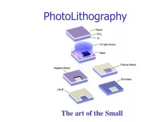
PhotoLithography
PhotoLithography. The art of the Small. Photolithography. • Photo-litho-graphy: lati n: light-stone-writing • Photolithography: an optical means for transferring patterns onto a substrate. • Patterns are first transferred to an imagable photoresist layer .

PhotoLithography
E N D
Presentation Transcript
PhotoLithography The art of the Small
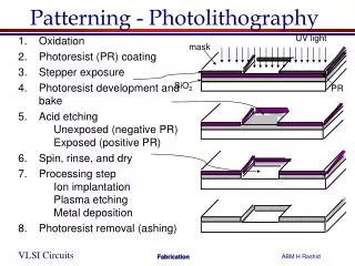
Photolithography • Photo-litho-graphy: latin: light-stone-writing • Photolithography: an optical means for transferring patterns onto a substrate. • Patterns are first transferred to an imagable photoresist layer. • Photoresist is a liquid film that is spread out onto a substrate, exposed with a desired pattern, and developed into a selectively placed layer for subsequent processing. • Photolithography is a binary pattern transfer: there is no gray-scale, color, nor depth to the image.
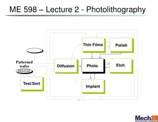
Overview of the Photolithography Process • Surface Preparation • Coating (Spin Casting) • Pre-Bake (Soft Bake) • Alignment • Exposure • Development • Post-Bake (Hard Bake) • Processing Using the Photoresist as a Masking Film • Stripping • Post Processing Cleaning (Ashing)
Basics of Photolithography for Processing • Microfabrication processes: – Additive ® deposition – Subtractive ® etching – Modifying ® doping, annealing, or curing • Two primary techniques for patterning additive and subtractive processes: – Etch-back: • photoresist is applied overtop of the layer to be patterned • unwanted material is etched away – Lift-off: • patterned layer is deposited over top of the photoresist • unwanted material is lifted off when resist is removed
Wafer Cleaning • Typical contaminants that must be removed prior to photoresist coating: • dust from scribing or cleaving (minimized by laser scribing) • atmospheric dust (minimized by good clean room practice) • abrasive particles (from lapping or CMP) • lint from wipers (minimized by using lint-free wipers) • photoresist residue from previous photolithography (minimized by performing oxygen plasma ashing) • bacteria (minimized by good DI water system) • films from other sources: – solvent residue – H 2O residue – photoresist or developer residue – oil – silicone
Wafer Priming • Adhesion promoters are used to assist resist coating. • Resist adhesion factors: • moisture content on surface • wetting characteristics of resist • type of primer • delay in exposure and prebake • resist chemistry • surface smoothness • stress from coating process • surface contamination • Ideally want no H 2O on wafer surface – Wafers are given a “singe” step prior to priming and coating 15 minutes in 80-90°C convection oven
Photoresist Spin Coating • Wafer is held on a spinner chuck by vacuum and resist is coated to uniform thickness by spin coating. • Typically 3000-6000 rpm for 15-30 seconds. • Resist thickness is set by: – primarily resist viscosity – secondarily spinner rotational speed • Resist thickness is given by t = kp 2 /w 1/2 , where – k = spinner constant, typically 80-100 – p = resist solids content in percent – w = spinner rotational speed in rpm/1000 • Most resist thicknesses are 1-2 mm for commercial Si processes.
Spinning Artifacts • Striations – ~ 30 nm variations in resist thickness due to nonuniform drying of solvent during spin coating – ~ 80-100 mm periodicity, radially out from center of wafer • Edge Bead – residual ridge in resist at edge of wafer – can be up to 20-30 times the nominal thickness of the resist – radius on wafer edge greatly reduces the edge bead height – non-circular wafers greatly increase the edge bead height – edge bead removers are solvents that are spun on after resist coating and which partially dissolve away the edge bead • Streaks – radial patterns caused by hard particles whose diameter are greater than the resist thickness
Prebake (Soft Bake) • Used to evaporate the coating solvent and to densify the resist after spin coating. • Typical thermal cycles: – 90-100°C for 20 min. in a convection oven – 75-85°C for 45 sec. on a hot plate • Commercially, microwave heating or IR lamps are also used in production lines. • Hot plating the resist is usually faster, more controllable, and does not trap solvent like convection oven baking.
Alignment and Exposure Hardware - 2 – For simple contact, proximity, and projection systems, the mask is the same size and scale as the printed wafer pattern. I.e. the reproduction ratio is 1:1. – Projection systems give the ability to change the reproduction ratio. Going to 10:1 reduction allows larger size patterns on the mask, which is more robust to mask defects. – Mask size can get unwieldy for large wafers. – Most wafers contain an array of the same pattern, so only one cell of the array is needed on the mask. This system is called Direct Step on Wafer (DSW). These machines are also called “Steppers” – Advantage of steppers: only 1 cell of wafer is needed – Disadvantage of steppers: the 1 cell of the wafer on the mask must be perfect-- absolutely no defects, since it gets used for all die.
Alignment and Exposure Hardware - 3 – Higher end research systems go one step further and use Direct Write on Wafer (DWW) exposure systems. – This can be accomplished using: • Excimer lasers for geometries down to 1-2 mm • Electron beams for geometries down to 0.1-0.2 mm • Focused ion beams for geometries down to 0.05-0.1 mm – No mask is needed for these technologies. – These are serial processes, and wafer cycle time is proportional to the beam writing time-- the smaller the spot, the longer it takes!
Mask to Wafer Alignment - 1 – 3 degrees of freedom between mask and wafer: (x,y,q) – Use alignment marks on mask and wafer to register patterns prior to exposure. – Modern process lines (steppers) use automatic pattern recognition and alignment systems. • Usually takes 1-5 seconds to align and expose on a modern stepper. • Human operators usually take 30-45 seconds with well-designed alignment marks.
Mask to Wafer Alignment - 2 • Normally requires at least two alignment mark sets on opposite sides of wafer or stepped region. • Use a split-field microscope to make alignment easier:
Optical Exposure • Projection Optics • Numerical Aperture • Raleigh Criterion • Coherence • Optical Correction & Phase Shift • Selection