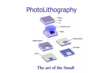
Advanced Photolithography
820 likes | 903 Vues
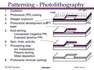
Advanced photolithography technology used in the sub-10nm wafer fabrication

Advanced Photolithography
E N D
Presentation Transcript
Discussion on Advanced Semiconductor Photolithographic Technologies Dr. Len Mei 2009/07/17 copy right by Dr. Len Mei 2017 1
Moore’s Law and Photolithography Moore’s Law is mostly enabled by photolithographic technology To print smaller feature size, light of smaller wavelength is needed to minimize light interference and diffraction. 2009/07/17 2
Number of transistors per area copy right by Dr. Len Mei 2017 4
Equations of photolithograpy NA is the numerical aperture n is the refraction index λ is the wavelength Θ is the maximum half focal point angle DOF is depth of focus к1 is a constant 0.4 Imax and Imin are the maximum and minimum intensity copy right by Dr. Len Mei 2017 5
Index of refraction n and wavelength λ Two ways to improve resolution: Make wavelength λsmaller Make n larger For air, n = 1 For water, n = 1.33 For oil, n = 1.52 λsmaller: 436 nm, 365 nm, 248 nm, 193 nm copy right by Dr. Len Mei 2017 6
Wavelength vs. technology Visible light 1:1 G-line 436 nm visible 5:1 G-line 436 nm 5:1 I-line 365 nm 4:1 KrF DUV 248 nm Deep UV ArF DUV 193 nm immersion invisible 157 nm EUV was abondaned. EUV 13.5 nm EUV 2009/07/17 copy right by Dr. Len Mei 200907 7
Spectrum Size of atom 0.3 nm Limit of semiconductor 3 nm Size of virus 100 nm EUV 13.5 nm DUV 248 nm, 193 nm i line 365 nm G line 436 nm copy right by Dr. Len Mei 2017 8
Wavelength to resolution ratio Wavelength 436 nm 365 nm 248 nm 193 nm 193 nm immersion 20 nm 13.5 nm Resolution 1 um 0.5 um 0.2 um 60 nm Ratio ~0.5 ~0.7 ~1.3 ~3 ~10 ~2 7 nm Wavelength must be smaller than the printed feature size. copy right by Dr. Len Mei 2017 9
Photolithographic technology development at user side (wafer fab) copy right by Dr. Len Mei 2017 10
Technologies to compensate wavelength longer than the dimension of patterns All other techniques to enhance resolution are generally known as Resolution Enhancement Technique (RET) RET above 60 nm Optical proximity correction (OPC) Off axis illumination (OAI) Phase shift mask (PSM) Hard mask (HM) 2009/07/17 11
Technologies to compensate wavelength longer than the dimension of patterns Below 60 nm, additional technologies are required: Double patterning (DP) Multiple patterning (MP) Restricted design rules (RDR) Gridded design rules (GDR) Source mask optimization (SMO) Inverse lithography technology (ILT) Negative tone development (NTD) 2009/07/17 12
Optical Proximity Correction OPC is an enhancement technique to compensate for image errors due to diffraction or process effects. OPC technique is to correct the shape of pattern on the mask by moving edges or adding extra polygons to the pattern, so that the printed pattern will have the desired shape. 2009/07/17 13
Effect of OPC Pattern on mask vs. pattern printed with and without OPC Pattern on mask Printed pattern Without OPC Wit OPC 2009/07/17 14
Rule based and model based OPC In earlier days, OPC is done by look-up tables based on width and spacing between features (rule based OPC). More sophisticated OPC technique uses models to simulate the final pattern and thereby drive the movement of edges to find the best solution. (model based OPC). However, below 60 nm, these techniques are no longer sufficient. 2009/07/17 15
Computational OPC At smaller geometry, the pattern distortion may depend on not only the pattern itself, but also the environment the pattern is in. For example, the pattern in densely populated area may exhibit different pattern behavior than sparsely populated area. The computational OPC simulates the actual lithographic process to obtain the final developed polygons on wafer, then feedback the simulation results to apply OPC on the mask. With computational OPC, full chip lithography simulation is possible. 2009/07/17 16
Computational OPC loop OPC input Mask System parameters Optical system simulation Resist system Etched system 2009/07/17 17
Source Mask Optimization SMO is a new computational OPC. It is a full chip mask synthesis solution. It is to optimize mask patterns in conjunction with illumination patterns by using algorithmic routines and linear optimization capabilities to generate a custom illumination source and a reticle. It takes into account of the parameters of lithography scanners needed to ensure manufacturability. SMO greatly extended the capability of immersion scanner beyond 22 nm. 2009/07/17 18
Feedback loop copy right by Dr. Len Mei 2017 20
Process spec vs. control limit Control limit – determined by equipment Spec limit defined by design copy right by Dr. Len Mei 2017 21
Process window Acceptable process distribution = process window copy right by Dr. Len Mei 2017 22
Inverse Lithography Technology Inverse Lithography Technology is to design the mask by starting from perfect pattern on wafer and work backwards to incorporating all the system introduced variations to be eliminated at the mask. It requires extensive computation and full characterization of the photolithographic process, scanner, photoresist and mask. copy right by Dr. Len Mei 2017 23
Off-Axis Illumination In an OAI optical system, the incoming light strikes the mask at an angle allowing some higher order diffracted light to be captured. It improves resolution and depth of focus. OAI is done using different arrangement of light sources OAI 24
Off-Axis Illumination The principle of OAI can be understood in the following illustration. The beam from 1 to - 1 is tilted so that beam 1 and 0 form the image. The spread is smaller therefore, it has better depth of focus. Beams 1 &-1 form image. Beams 1 & 0 form image. 25
Effect of OAI on image contrast Contrast=(Imax-Imin)/(Imax+Imin) = normalized ΔI Normalized image log slope λ CD (nm) copy right by Dr. Len Mei 2017 26
Phase Shift Mask PSM’s use the interference generated by light wave phase differences through different mask thickness to improve resolution. There are two types of PSM: Alternating Attenuated In alternating phase-shift masks, certain transmitting regions are made thinner or thicker so that the light traveling through adjacent paths shift phase by 180 degree, thus having the effect of improving the contrast and the resolution. Plot of scattered light (normalized to incident light) as a function of the phase of a phase edge. 27
Phase Shift Mask In an attenuated phase-shift masks, The light- blocking parts of the mask are modified to allow a small amount of light to be transmitted through. That light is not strong enough to print a pattern on the wafer, but it can interfere with the light coming from the transparent parts of the mask. 2009/07/17 28
No PSM Alternating PSM Attenuated PSM copy right by Dr. Len Mei 2017 29
Out of phase light cancels each other (a) Alternating PSM Thin MoSi patterns shift phase by 180o Transmitted light cancels out diffracted light (b) Attenuated PSM copy right by Dr. Len Mei 2017 30
Attenuated PSM Fully transmitted light 180o out of phase light cancel each other Partially transmitted light The resultant wave copy right by Dr. Len Mei 2017 31
Double Patterning and Multi- Patterning DP and MP arelithographic techniques to improve the resolution by more than one exposure (pitch splitting technique) or to use the etched feature to form sidewalls (spacer technique). Pitch splitting technique involves the division of a pattern into two or three parts, each of them processed separately, in the litho-etch-litho-etch sequence, also known as LELE. 2009/07/17 32
Double Patterning and Multi- Patterning As shown below, the patterns of the same color are printed and etched together. It takes three print and etch processes to complete (triple patterning) . copy right by Dr. Len Mei 2017 33
Double Patterning and Multi- Patterning using Hard Mask A different technique involves a hard mask. In step one, the pattern on photoresist is transferred to an underlying hardmask layer. The exposed photoresist is then removed and a second photoresist is applied. It goes through another exposure and etch. Hard mask materials have much higher etch selectivity than photoresist. That is, it etches much slower than photoresist in the etching of substrate material. It needs high tensile stress and high film density, such as amorphous carbon, TiN, silicon nitride, silicon oxynitride, oxide, spin-on carbon etc. copy right by Dr. Len Mei 2017 34
Double Patterning and Multi- Patterning using spacer Spacer technique is a self-aligned technique. The sidewalls of an etched pattern form the desirable structure. Simple spacer technique is called SADP (Self-Aligned Double Patterning), as shown on the left. More complicated technique is called SAQP (Self- Aligned Quadruple Patterning), which repeats SADP a second time. copy right by Dr. Len Mei 2017 35
Double Patterning and Multi- Patterning involve design As one can imagine, the use of DP and MP involves not only the process change but also extensive work in design. The steps involved are: design of DP or MP compliant layout; design verification; decomposition of the layout into double or triple layers OPC steps for each layer OPC verification for each layer mask data preparation mask manufacture finally processing in the fab, each of these process step needs to be developed and controlled just like any other process step. copy right by Dr. Len Mei 2017 36
Double Patterning and Multi- Patterning involve design It introduced many unfavorable factors into the process. Cost in more processing steps, more masks, in design, layout, verification and mask design Alignment Process variability. Cycle time Testing and debugging Process tolerance Additional difficulties are found in design and mask synthesis (decomposition, RET, OPC and verification) for compliant layouts. copy right by Dr. Len Mei 2017 37
Restricted Design Rules Today, design rules are the only rules designers need to follow for the physical design and layout. However, increasing variability in the performance of the device requires more rules to be imposed. For example: Lithographic rounding of the active and the contact in a source or drain connection can reduce the alignment marginality In a gate, horizontal bends in the poly nearby can induce a variation in the L-effective. A curvature in the horizontal-to-vertical transition in the active layer can cause variation in the W-effective. copy right by Dr. Len Mei 2017 38
Restricted Design Rules RDR imposes additional restrictions to the existing design rules. RDR is based on the concept that a regular array is significantly easier to manufacture than a random array of cells. RDR is a new way of thinking of the design-for- manufacturability (DFM). So far, it is aimed at layout rather than design. It makes changes in physical design like place-and- route. But long term wise, new EDA tools, process equipment or design methodologies will emerge. copy right by Dr. Len Mei 2017 39
Restricted Design Rules Restrictive Design Rules and Their Impact on 22 nm Design and Physical Verification David Abercrombie, Mentor Graphics Corporation Praveen Elakkumanan, IBM copy right by Dr. Len Mei 2017 40
Gridded Design Rules GDR is a special set of the Restricted Design Rules. As the name implies, the layout is divided into grids, such as Layout Base Unit (LBU) Grid, Placement Grid. The layout objects are line (poly, metal), point (contact, via), block (diffusion, implant). All objects need to have vertices on the LBU grids and anchors (center line of line object, center of point object, edges of block object) on the Placement grids. Following GDR, the layout will be much more regular and comply to higher DFM. copy right by Dr. Len Mei 2017 41
Negative Tone Development In a NTD, the negative tone resist (NTR) is used, where the exposed resist is polymerized and becomes insoluble to the developer. Masks used for negative photoresists contain the inverse or photographic "negative" of the pattern. In the early days of the industry, NTR was widely used. It gradually phased out because of its poor resolution at smaller feature sizes due to the exposed and unexposed areas permeated by the solvent causing pattern distortions. However, the effect of NTD and PTD (Positive Tune Development) are not complimentary. This opens up a window for optimizing the resist system. copy right by Dr. Len Mei 2017 42
Difference between PTR and NTR The area exposed in the positive resist is removed, while the area exposed in the negative resist stays. PTR NTR Red materials stay after development. copy right by Dr. Len Mei 2017 43
Negative Tone Development With the advance in negative tone development technology, the industry has found renewed interest in the NTD. NTR can print isolated and densely packed lines at the same line width, while PTR has up to 10% of nominal line width due to the imaging property of lens. NTR also provides advantages to the isofocus bias – the variation in CD due to exposure and focus combination. NTR provides low swelling and smooth- dissolving behavior during development, therefore, better line edge roughness (LER). Due to the above advantages, NTR is superior in double patterning process. copy right by Dr. Len Mei 2017 44
Negative Tone Development NTR processing such as the pre-applied bake (PAB) temperature, post-exposure bake (PEB) temperature, development procedure, and rinse procedure are very effective for improving the lithographic performance. NTR enables the printing of dark field features on wafer using bright field masks with a better manufacturing capability for back-end-of-line processing. However, NTR is not cure for all. For example, for contact layer, NTR has smaller depth of focus. The ability to choose the right tone may play an important role in optimizing the process. copy right by Dr. Len Mei 2017 45
Technology development at equipment vendor side copy right by Dr. Len Mei 2017 46
Evolution of Photolithography tools Effort to improve resolution. Change of wavelength is no trivial task… Change in optics Change in photoresist system Change in mask system 2009/07/17 47
Theoretically, To improve resolution, we need to Reduce wavelength (248 nm , 193 nm, 13.5 nm) Increase refraction index (air to water) Increase focal point angle (OAI) To improve depth of focus, we need to Increase refraction index Increase focal point angle To improve contrast, we need to Widen minimum to maximum intensity At the same time, we have to achieve Overlay requirement: 20% of half pitch CD uniformity: 7% of half pitch copy right by Dr. Len Mei 2017 48
Immersion scanner copy right by Dr. Len Mei 2017 49
Immersion scanner copy right by Dr. Len Mei 2017 50