Download
1 / 6
60 likes | 389 Vues
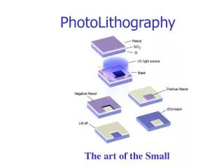
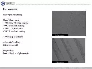
Previous week Microgap patterning Photolithography - 4000rpm 40s spin-coating - 90C 1min soft baking - 3min UV irradiation - 90C 1min hard baking ~10um gap is defined After AZO etching, PR is peeled off Suspection : Poor adhesion of photoresist. Before etching. After etching.

E N D
Previousweek Microgap patterning Photolithography - 4000rpm 40s spin-coating - 90C 1min soft baking - 3min UV irradiation - 90C 1min hard baking ~10um gap is defined After AZO etching, PR is peeled off Suspection: Poor adhesion of photoresist Before etching After etching
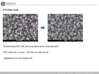
Thisweek Result of 14.5h Lateral growth → Indicates overgrowth into microgap region (~8um width) Low coverage caused by AZO undercut below PR (PR is intentionally not removed for clean AZO surface after entire process) ① After AZO etching ②After ZnO growth
Thisweek PR adhesion is improved (HMDS treatment, 110ºC soft baking) Remaining ssues ① AZO undercut Our AZO film is relatively thick (800nm) Isotropic etching is severe ② PR Curing Metal halide lamp generates too much heat → Difficult to obtain optimum curing Mercury lamp: Insufficient power 30min, 1hr, 2hr curing is failed complete curing →
Next week • Photolithography • UV curing lamp setup • Diluted etchant or TMAH etching • CIGS • Uniformity issue • Plasma scan on 5cm x 5cm substrate Plasma scan Heat Substrate Metal support
Carbon nanotube TFT Semiconductor-Metallic separation ① Main difference: Electronic property ② Goal: Positional saparation → Electromechanical driving can be appropriate mean ex) electropropulsion of nanowire diode (not an electrophoresis) Nanodiode PS particle
Carbon nanotube TFT ex) Separation of metallic CNT from source/drain by using electromagnetic force F ① Given electric and magnetic field, only metallic CNT is forced Compete with Van der Waals force I B ②Using UV resin to ‘float’ metallic CNT Curing resin for permanently separate CNT from source/drain UV UV resin