Previous week
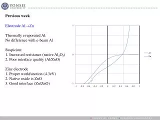
Previous week. Electrode Al→Zn Thermally evaporated Al: No difference with e-beam Al Suspicion: 1. Increased resistance (native Al 2 O 3 ) 2. Poor interface quality (Al/ ZnO ) Zinc electrode 1. Proper workfunction (4.3eV) 2. Native oxide is ZnO 3. Good interface (Zn/ ZnO ).

Previous week
E N D
Presentation Transcript
Previousweek Electrode Al→Zn Thermally evaporated Al: No difference with e-beam Al Suspicion: 1. Increased resistance (native Al2O3) 2. Poor interface quality (Al/ZnO) Zinc electrode 1. Proper workfunction (4.3eV) 2. Native oxide is ZnO 3. Good interface (Zn/ZnO)
Previous week ① Efficiency goal : ~1.2% (Zn back contact), ~0.9% (ITO back contact) ② Folded cell ③ Cell on paper substrate ④ Analysis of metal back contact (What is difference between Al and Zn electrode?) WO3/Ag/WO3 P3HT/PCBM ITO/ZnO PET
This week Efficiency enhanced (0.17% → 0.39%) Many failed cell (Electrode short) Low VOC and FF (Low shunt resistance) Suspicion: Non-uniform zinc surface Direct contact of active layer & zinc bottom electrode Low reflectivity of zinc electrode
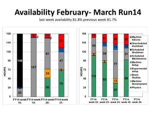
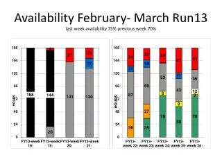
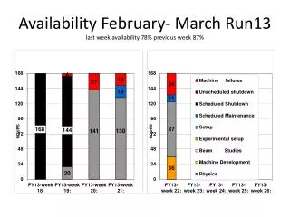
This week Zinc deposition Thermal evaporation failed: Chamber wall and quartz crystal is coated But, no zinc coating on substrate (?) Zinc is deposited by RF sputtering: Cloudy gray film is appeared (Rough and porous surface) Blue-gray appearance: incorporation of zinc oxide (Ref. Characterization of mixed zinc-oxidized zinc thin films deposited by a cold remote nitrogen plasma) Blue-gray color of sputtering target surface (Corroded by reactive sputtering?) → Target grinding is required
This week S-shape I-V characteristic at Al bottom electrode configuration Compared to reference, (JAP) S-shape kink is located at (-) and higher voltage
This week In reference, S-shape kink is explained by interface dipole (at metal-like PEDOT/Bathocuprine interface) Interface dipole at Al/ZnO? → Can be confirmed by photoemission spectroscopy
This week S-shape curve is at 3rd quadrant Interface dipole has to be located like: - + WO3 Ag WO3 P3HT/PCBM ZnO Al - + - + - + - + - + - + - + - + In this explanation, injection barrier is decreased. But in experiment, current increases at very high voltage (>3V) → Cannot be explained (Large electron barrier at cathode?)
Next week ① Continue efficiency improvement - Electric field and barrier consideration ② Continue theoretical analysis aluminum electrode cell - Electric field and barrier consideration ③ Device fabrication on ITO-PET - Folded cell fabrication
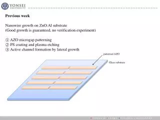
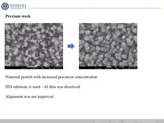
Previous week Step #1 Step #2 Poor Align No lateral growth
Previous week Field-assisted ZnOnanowire growth -2.0V potential Ag catalyst (on glass) (-) (+) 1. Highly-aligned vertical growth 2. Without (sputtered) ZnO seed layer 3. Fast growth Silicon wafer Ag/Al on Glass ZnOnanowire Al,Ag deposition on glass
Previous week ① SEM work to confirm nanorod and film morphology ② Continue to TPT filling and plasma etching experiment ③ Lateral overgrowth experiment ④ Nanowire growth time optimization → Shorter process time
This week Field-assisted growth: Dense & better align
This week 2nd step growth: Film formation
This week (Ref.) 0.5mmol zinc nitrate, HMTA 80℃, 5hours Silver catalyst -2.0V potential 10mmol zinc nitrate, HMTA 90℃, 2hours Silicon substrate -1.2V potential (!) Ag/ZnO is not ohmic contact Zn seed layer is considered: Ohmic contact, High nucleation density → Zn seed layer is dissolved during hydrothermal growth
This week Vertical growth during 2nd growth step Suspicion: (-) charges on (0001) plane at pH 10.9 (Optimum pH 10.5~10.9 by reference) prohibits surface passivation by citrate ions TPT filling ZnOnanowire growth PDMS cover TPT filling from side Removing PDMS
Next week Nanowire aligning → More precursor concentation (higher nucleation density) →Higher growth temperature Ohmic contact →ZnO growth on Al, ITO Vertical growth during 2nd growth step →ZnO lateral growth at pH 10.5 TPT filling →Plasma etching → Lateral growth from revealed nanowire heads → Confirm by SEM