Nanowire Growth Challenges and Strategies: Transitioning from ITO to ZnO:Al Substrates
This week, we encountered several setbacks in our nanowire growth experiments. Increased precursor concentration on ITO substrates did not yield expected results, with attempts at PDMS contact and plasma etching failing. Switching to spin coating with polystyrene/toluene did not improve outcomes. Despite increasing applied voltage, nanowire alignment remains unacceptable. We plan to transition to ZnO:Al substrates next week, focusing on AZO microgap patterning, PS coating, plasma etching, and lateral growth to enhance our results.

Nanowire Growth Challenges and Strategies: Transitioning from ITO to ZnO:Al Substrates
E N D
Presentation Transcript
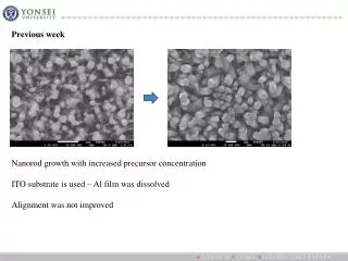
Previous week Nanorod growth with increased precursor concentration ITO substrate is used – Al film was dissolved Alignment was not improved
Previous week TPT overcoat – PDMS conformal contact failed Plasma etching failed to reveal nanorod heads 2nd growth step is also failed
This week TPT injection is not worked because of large particles → Spincoating (Polystyrene/Toluene) is used Plasma etching : failed (sample too close to electrode)
This week Nanowire height is increased ~3x as applied voltage increased from -1.2V to 2.0V Still insufficient to good align (>10um length is required) -1.2V 80C ~1.5um -2.0V 80C ~4.4um
This week Nanowire growth with volage over -2.0V → Nanowires are shorten ITO glass is not appropriate for nanowire growth (No good result without additional seed layer in references) -2.6V 80C -2.3V 80C -2.0V 80C (All picture x15000)
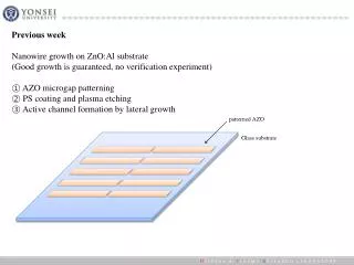
Next week Nanowire growth on ZnO:Al substrate (Good growth is guaranteed, no verification experiment) ① AZO microgap patterning ② PS coating and plasma etching ③ Active channel formation by lateral growth patterned AZO Glass substrate
Zinc deposition Large surface roughness (induces shunt resistance)