Top Down Method Photolithography Basics
320 likes | 881 Vues
Top Down Method Photolithography Basics.

Top Down Method Photolithography Basics
E N D
Presentation Transcript
Top Down MethodPhotolithography Basics Author’s Note: Significant portions of this work have been reproduced and/or adapted with permission from material created by the Maricopa Advanced Technology Education Center, part of the Academic Affairs Division, Maricopa Community College District.
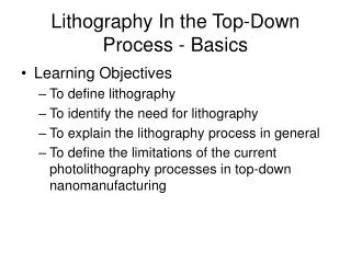
Lithography In the Top-Down Process - Basics • Learning Objectives • To define lithography • To identify the need for lithography • To explain the lithography process in general • To define the limitations of the current photolithography processes in top-down nanomanufacturing
What is Lithography? • Lithography is a process that uses focused radiant energy and chemical films that are affected by this energy to create precise temporary patterns in silicon wafers or other materials. • Lithography is an important part of the top- down manufacturing process, since these temporary patterns can be used to add or remove material from a given area
What is Lithography (2)? • Lithography is one of the 4 major processes in the top-down model • Lithography • Etching • Deposition • Doping • In order to perform the other 3 processes, we must precisely define where to do them • Lithography Does This!
Lithography’s Key Role in the Process • With multiple etch, deposition, and doping processes taking place in the fabrication of a device, the lithography process is repeated many times. • The precision and accuracy of lithography in the manufacturing process controls, to a first degree, the success in building a device.
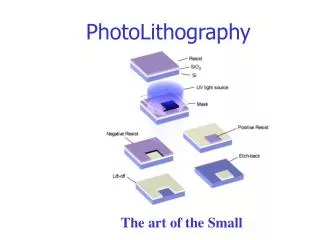
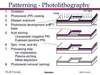
Overview of the Photolithography Process • Photolithography uses light energy passing through a patterned mask • The light is focused onto the photosensitive surface • Chemical changes in the surface coating occur • Subsequent chemical development creates a temporary pattern on the surface. From MATEC Module 40
Steps in the Lithography Process • Silicon wafers are commonly used substrates in the top- down process. • The first step is to coat the clean surface of the wafer with a light sensitive chemical emulsion known as photoresist Photoresist Dispensing (Spinners) (MATEC Module 40)
Steps in the Lithography Process • Baking the resist causes it to form a solid layer. • The chemical properties of the photoresist define what wavelengths of light will affect it. Photoresist Dispensing (Spinners)
Steps in the Lithography Process(2) • A photomask, typically made of quartz with a chrome plating controls where the radiant energy will strike the photoresist. • Photomasks can be made with electron beam patterning tools to create fine features Exposure
Practice Questions Click once for each question. 1. Define lithography. The Art and science of defining patterns of features on a wafer. 2. How are photography and photolithography similar? Both processes involve exposing an image onto a chemically treated surface. Both processes involve depositing chemicals on the surface, exposing the surface to light, and developing the surface to reveal the image. 3. What is the goal of photolithography? To define patterns of features on a wafer in preparation for further processing.
Steps in the Lithography Process(3) - Exposure Exposure • Exposure of the photoresist to the radiant energy pattern occurs next • There are several ways to do this • Contact/proximity printing • Projection printing (shown here) • Projection scanning
Contact Printing • The mask is directly in contact with the wafer • Advantages • Simple • Low Cost • Disadvantages • Poor for small features • Mask damage may occur from contact • Defects from contaminants on mask or wafer due to contacting surfaces From MATEC Module 40
Proximity Printing • The mask is above the wafer surface • Advantages • Mask damage is minimal • Good registration possible • Disadvantages • Poorer resolution due to distance from the surface • Defects from contaminants on mask or wafer due to contacting surfaces • Diffraction errors
Projection Printing (1) • An optical system focuses the light source and reduces the mask image for exposure on the surface • Advantages • Higher resolution • Lens system reduces diffraction error • Disadvantages • Errors due to focus of lens system may occur • Limiting factor in resolution can be due to optical system From MATEC Module 40
Projection Printing (2) • Step and repeat aligner • Lens reduction • Good throughput but resolution limited to about 0.35 uM • Cadiotropic System • Mirror, folding prisms and lenses 1:1 ratio • Less common than steppers From MATEC Module 40
Step and Scan Aligner • Uses a spherical mirror and a scanning pattern • Advantages • Improved throughput • Lens system aberration minimized • Disadvantages • Complex motion system is required for alignment and precise tracing • Light source wavelength is still an factor limiting feature size
Diffraction • As feature sizes shrink in the mask, the wavelength of the light used as a source becomes a factor. • Shrinking feature sizes require shorter wavelengths of light • The photoresist must be optimized to match the light source used. From MATEC Module 40
Ultraviolet Sources • The traditional mercury vapor lamp has peaks in certain ranges. • The intensity of some UV peaks is low • The photoresist must be optimized to match the light source used. From MATEC Module 40
Practice Questions Click once for each question. 1. Which process puts the mask on the wafer? Contact lithography. 2. What effect creates a “haze” around a mask pattern when feature sizes become smaller? Diffraction 3. Which process uses a lens to reduce mask feature sizes? Projection Lithography 4. Besides wavelength, what limits feature sizes? Numerical Aperture of the lens
Sources and References [1] Maricopa Advanced Techology Education Center (2001) Module 40 The Photolithography Process [2] Chang, C.Y., & Sze, S. M. (1996). ULSI technology. New York: McGraw Hill. [3] Garza-Lopez, T., & Sancaktar, E. (2002) Excimer lasers, how they work and ablate. Vacuum and Coating Technology, 3, 52-59. [4] Hand, A. (2002) NGL: Forever next generation? Semiconductor International, 25, 57-64. [5] Quirk, M., & Serda, J. (2001) Semiconductor manufacturing technology. Upper Saddle River, NJ: Prentice Hall. [6] Van Zant, P. (2000). Microchip fabrication: A practical guide to semiconductor processing (4th ed.). New York: McGraw Hill. [7] Wolf, S., & Tauber, R. N. (1986). Silicon processing the VLSI era. (vol. 1). Sunset Beach, CA: Lattice Press. [8] Xiao, H. (2001). Introduction to semiconductor manufacturing technology. Upper Saddle River, NJ: Prentice-Hall. [9] Bohr, M.T. (2006) “Intel’s Silicon R&D Pipeline, Intel Developer Forum, Moscow, April 26, 2006 [10] Brunner, Gil, Fonseca, and Seoung (2004) “New Opportunities for Semiconductor Manufacturing”, 2004 Immersion and 157nM Symposium, Sematech, August 3, 2004 [11] Sematech News, 21 May, 2007, International Sematech http://www.sematech.org/corporate/news/releases/20070521.htm [12] Peters, Lauren (2008) “32nM Marked by Litho, Transistor Changes”, Semiconductor International http://www.semiconductor.net/article/CA6515401.html?nid=3656 [13] R. S. Dhaliwal, W. A. Enichen, S. D. Golladay, M. S. Gordon, R. A. Kendall, J. E. Lieberman, H. C. Pfeiffer, D. J. Pinckney, C. F. Robinson, J. D. Rockrohr, W. Stickel, and E. V. Tressler PREVAIL—Electron Projection Technology Approach for Next-Generation Lithography,IBM Journal of Research and Development V.45 #5 (2001)