Photolithography
Photolithography. Outline. Motivation History Photolithography Methods and Theories Preparation and Priming Spin-Coating Photoresists Soft-baking Mask Alignment and Exposure Developing Hard-baking References. Motivation. Key top-down manufacturing technology Applications:

Photolithography
E N D
Presentation Transcript
Outline • Motivation • History • Photolithography • Methods and Theories • Preparation and Priming • Spin-Coating • Photoresists • Soft-baking • Mask Alignment and Exposure • Developing • Hard-baking • References
Motivation • Key top-down manufacturing technology • Applications: • Microelectronics (ICs, transistors, etc.) • Microelectromechanical Systems (MEMS) • Sensors
History • Historically, lithography is a type of printing technology that is based on the chemical repellence of oil and water. • Photo-litho-graphy: latin: light-stone-writing • In 1826, Joseph Nicephore Niepce, in Chalon, France, takes the first photograph using bitumen of Judea on a pewter plate, developed using oil of lavender and mineral spirits • In 1935 Louis Minsk of Eastman Kodak developed the first negative photoresist • In 1940 Otto Suess developed the first positive photoresist. • In 1954, Louis Plambeck, Jr., of Du Pont, develops the Dycryl polymeric letterpress plate
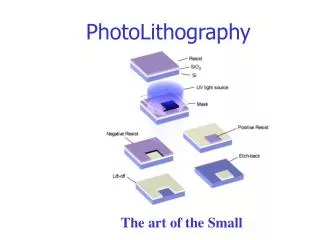
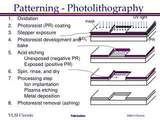
Photolithography • In photolithography, the pattern is created photographically on a substrate (silicon wafer) • Photolithography is a binary pattern transfer: there is no gray-scale, color, nor depth to the image • This pattern can be used as a resist to substrate etchant, or a mold, and other forms of design processes • The steps involved are wafer cleaning, photoresist application, soft baking, mask alignment, and exposure and development
Preparation and Priming • Prepare the substrate (silicon wafer): • Wash with appropriate solvent to remove any matter and other impurities • TCE, Acetone, MeOH • Dry in Oven at 150°C for 10 min. • Place on hotplate and cover with petri dish, let temp. stabilize at 115°C. • Deposit Primer (optional) • Chemical that coats the substrate and allows for better adhesion of the resist TCE = trichloroethylene, MeOH = methanol
Spin-Coating the Resist • Deposit a layer of SiO2 (silicon dioxide) on the surface of the wafer to serve as a barrier. • Spin on the photoresist to the surface of the wafer • Standard methods are to use high spin coaters • RPM: • Time: • Produces a thin uniform layer of photoresist on the wafer surface. • Use red/amber light at this stage
Photoresist • Photoresist is an organic polymer which changes its chemical structure when exposed to ultraviolet light. • It contains a light-sensitive substance whose properties allow image transfer onto a printed circuit board. • There are two types of photoresist: positive and negative
Diagram: • Exposure to UV light causes the resist to polymerize, and thus be more difficult to dissolve • Developer removes the unexposed resist • This is like a photographic negative of the pattern • Exposure to UV light makes it more soluble in the developer • Exposed resist is washed away by developer so that the unexposed substrate remains • Results in an exact copy of the original design
Soft-Baking • Put on hotplate, or in oven • Temperature: , Time: • Removes volatile solvents from the coating • Makes photoresist non-sticky • Hardens to amorphous solid • Be careful not to overbake and destroy the sensitizer
Mask Alignment and Exposure • Photomask is a square glass plate with a patterned emulsion of metal film on one side • After alignment, the photoresist is exposed to UV light • Three primary exposure methods: contact, proximity, and projection
Photoresist Developer • Highly-pure buffered alkaline solution • Removes proper layer of photoresist upon contact or immersion • Degree of exposure affects the resolution curves of the resist
Hard Baking • Final step in the photolithographic process • Not always necessary; depends on the resist • Hardens the photoresist • Improves adhesion of the photoresist to the wafer surface
References • Motivation • http://www.mems-issys.com/html/singlestep.html#photolithography • http://www.chipcenter.com/columns/bmcginty/col005.html • http://www.adhesives.de/seiten/literature_highlights/gaynes.htm • Background • http://www.lib.udel.edu/ud/spec/exhibits/color/lithogr.htm • http://www.ee.washington.edu/research/microtech/cam/PROCESSES/PDF%20FILES/Photolithography.pdf • http://www.dbanks.demon.co.uk/ueng/plith.html • Theories and Methods • http://www.ece.gatech.edu/research/labs/vc/theory/PosNegRes.html • http://www.ece.gatech.edu/research/labs/vc/theory/photolith.html • http://www.intl-light.com/photoresist.html