Chapter 6 Photolithography
Chapter 6 Photolithography. Hong Xiao, Ph. D. hxiao89@hotmail.com www2.austin.cc.tx.us/HongXiao/Book.htm. Objectives. List the four components of the photoresist Describe the difference between +PR and - PR Describe a photolithography process sequence

Chapter 6 Photolithography
E N D
Presentation Transcript
Chapter 6 Photolithography Hong Xiao, Ph. D. hxiao89@hotmail.com www2.austin.cc.tx.us/HongXiao/Book.htm www2.austin.cc.tx.us/HongXiao/Book.htm
Objectives • List the four components of the photoresist • Describe the difference between +PR and -PR • Describe a photolithography process sequence • List four alignment and exposure systems • Describe the wafer movement in a track-stepper integrated system. • Explain relationships of resolution and depth of focus to wavelength and numerical aperture. www2.austin.cc.tx.us/HongXiao/Book.htm
Introduction Photolithography • Temporarily coat photoresist on wafer • Transfers designed pattern to photoresist • Most important process in IC fabrication • 40 to 50% total wafer process time • Determines the minimum feature size www2.austin.cc.tx.us/HongXiao/Book.htm
Applications of Photolithography • Main application: IC patterning process • Other applications: Printed electronic board, nameplate, printer plate, and et al. www2.austin.cc.tx.us/HongXiao/Book.htm
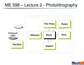
e-Beam or Photo EDA PR Chip Photolithography Ion Implant Mask or Reticle Etch IC Fabrication EDA: Electronic Design Automation PR: Photoresist www2.austin.cc.tx.us/HongXiao/Book.htm
Materials Etch PR strip Test Wafers Photo-lithography Thermal Processes Dielectric deposition Packaging Masks Implant PR strip CMP Final Test IC Design IC Processing Flow IC Fab Metallization www2.austin.cc.tx.us/HongXiao/Book.htm
Photolithography Requirements • High Resolution • High PR Sensitivity • Precision Alignment • Precise Process Parameters Control • Low Defect Density www2.austin.cc.tx.us/HongXiao/Book.htm
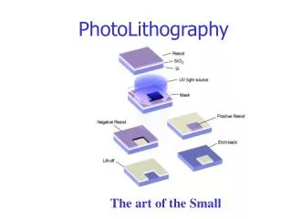
Photoresist • Photo sensitive material • Temporarily coated on wafer surface • Transfer design image on it through exposure • Very similar to the photo sensitive coating on the film for camera www2.austin.cc.tx.us/HongXiao/Book.htm
Photoresist Negative Photoresist • Becomes insoluble after exposure • When developed, the unexposed parts dissolved. • Cheaper Positive Photoresist • Becomes soluble after exposure • When developed, the exposed parts dissolved • Better resolution www2.austin.cc.tx.us/HongXiao/Book.htm
Negative and Positive Photoresists Photoresist Substrate UV light Mask/reticle Photoresist Exposure Substrate Negative Photoresist Substrate After Development Positive Photoresist Substrate www2.austin.cc.tx.us/HongXiao/Book.htm
Photoresist Chemistry • Start with printed circuit • Adapted in 1950 in semiconductor industry • Critical to the patterning process • Negative and positive photoresist www2.austin.cc.tx.us/HongXiao/Book.htm
Photoresist Composition • Polymer • Solvents • Sensitizers • Additives www2.austin.cc.tx.us/HongXiao/Book.htm
Polymer • Solid organic material • Transfers designed pattern to wafer surface • Changes solubility due to photochemical reaction when exposed to UV light. • Positive PR: from insoluble to soluble • Negative PR: from soluble to insoluble www2.austin.cc.tx.us/HongXiao/Book.htm
Solvent • Dissolves polymers into liquid • Allow application of thin PR layers by spinning. www2.austin.cc.tx.us/HongXiao/Book.htm
Sensitizers • Controls and/or modifies photochemical reaction of resist during exposure. • Determines exposure time and intensity www2.austin.cc.tx.us/HongXiao/Book.htm
Additives • Various added chemical to achieve desired process results, such as dyes to reduce reflection. www2.austin.cc.tx.us/HongXiao/Book.htm
Negative Resist • Most negative PR are polyisoprene type • Exposed PR becomes cross-linked polymer • Cross-linked polymer has higher chemical etch resistance. • Unexposed part will be dissolved in development solution. www2.austin.cc.tx.us/HongXiao/Book.htm
Negative Photoresist Mask Negative Photoresist Expose Development www2.austin.cc.tx.us/HongXiao/Book.htm
Negative Photoresist Disadvantages • Polymer absorbs the development solvent • Poor resolution due to PR swelling • Environmental and safety issues due to the main solvents xylene. www2.austin.cc.tx.us/HongXiao/Book.htm
Comparison of Photoresists - PR + PR Film Film Substrate Substrate www2.austin.cc.tx.us/HongXiao/Book.htm
Positive Photoresist • Exposed part dissolve in developer solution • Image the same that on the mask • Higher resolution • Commonly used in IC fabs www2.austin.cc.tx.us/HongXiao/Book.htm
Positive Photoresist • Novolac resin polymer • Acetate type solvents • Sensitizer cross-linked within the resin • Energy from the light dissociates the sensitizer and breaks down the cross-links • Resin becomes more soluble in base solution www2.austin.cc.tx.us/HongXiao/Book.htm
Question • Positive photoresist can achieve much higher resolution than negative photoresist, why didn’t people use it before the 1980s? • Positive photoresist is much more expensive therefore negative photoresist was used until it had to be replaced when the minimum feature size was shrunk to smaller than 3 mm. www2.austin.cc.tx.us/HongXiao/Book.htm
Chemically Amplified Photoresists • Deep ultraviolet (DUV), l 248 nm • Light source: excimer lasers • Light intensity is lower than I-line (365 nm) from high-pressure mercury lamp • Need different kind of photoresist www2.austin.cc.tx.us/HongXiao/Book.htm
Chemically Amplified Photoresists • Catalysis effect is used to increase the effective sensitivity of the photoresist • A photo-acid is created in PR when it exposes to DUV light • During PEB, head-induced acid diffusion causes amplification in a catalytic reaction • Acid removes protection groups • Exposed part will be removed by developer www2.austin.cc.tx.us/HongXiao/Book.htm
Chemically Amplified Photoresist Before PEB After PEB Exposed PR Exposed PR Heat + H + + H + + Protecting Groups Protecting Groups www2.austin.cc.tx.us/HongXiao/Book.htm
Requirement of Photoresist • High resolution • Thinner PR film has higher the resolution • Thinner PR film, the lower the etching and ion implantation resistance • High etch resistance • Good adhesion • Wider process latitude • Higher tolerance to process condition change www2.austin.cc.tx.us/HongXiao/Book.htm
Photoresist Physical Properties • Photoresist must be able to withstand process conditions • Coating, spinning, baking, developing. • Etch resistance • Ion implantation blocking www2.austin.cc.tx.us/HongXiao/Book.htm
Photoresist Performance Factor • Resolution • Adhesion • Expose rate, Sensitivity and Exposure Source • Process latitude • Pinholes • Particle and Contamination Levels • Step Coverage • Thermal Flow www2.austin.cc.tx.us/HongXiao/Book.htm
Resolution Capability • The smallest opening or space that can produced in a photoresist layer. • Related to particular processes including expose source and developing process. • Thinner layer has better resolution. • Etch and implantation barrier and pinhole-free require thicker layer • Positive resist has better resolution due to the smaller size of polymer. www2.austin.cc.tx.us/HongXiao/Book.htm
Photoresist CharacteristicsSummary Parameter Negative Positive Polymer Polyisoprene Novolac Resin Polymerization Photo-solubilization Photo-reaction Provide free radicals Changes film Sensitizer for polymer cross-link to base soluble Additives Dyes Dyes www2.austin.cc.tx.us/HongXiao/Book.htm
Photolithography Process www2.austin.cc.tx.us/HongXiao/Book.htm
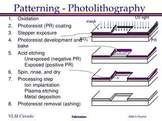
Basic Steps of Photolithography • Photoresist coating • Alignment and exposure • Development www2.austin.cc.tx.us/HongXiao/Book.htm
Basic Steps, Old Technology • Wafer clean • Dehydration bake • Spin coating primer and PR • Soft bake • Alignment and exposure • Development • Pattern inspection • Hard bake PR coating Development www2.austin.cc.tx.us/HongXiao/Book.htm
Basic Steps, Advanced Technology • Wafer clean • Pre-bake and primer coating • Photoresist spin coating • Soft bake • Alignment and exposure • Post exposure bake • Development • Hard bake • Pattern inspection PR coating Track-stepper integrated system Development www2.austin.cc.tx.us/HongXiao/Book.htm
Soft bake PEB Figure 6.5 Previous Process Surface preparation Clean PR coating Alignment & Exposure Hard bake Development Track system Photo cell Rejected Inspection Strip PR Photo Bay Approved Ion Implant Etch www2.austin.cc.tx.us/HongXiao/Book.htm
Wafer Clean Gate Oxide Polysilicon STI USG P-Well www2.austin.cc.tx.us/HongXiao/Book.htm
Pre-bake and Primer Vapor Primer Polysilicon STI USG P-Well www2.austin.cc.tx.us/HongXiao/Book.htm
Photoresist Coating Primer Photoresist Polysilicon STI USG P-Well www2.austin.cc.tx.us/HongXiao/Book.htm
Soft Bake Photoresist Polysilicon STI USG P-Well www2.austin.cc.tx.us/HongXiao/Book.htm
Alignment and Exposure Gate Mask Photoresist Polysilicon STI USG P-Well www2.austin.cc.tx.us/HongXiao/Book.htm
Alignment and Exposure Gate Mask Photoresist Polysilicon STI USG P-Well www2.austin.cc.tx.us/HongXiao/Book.htm
Post Exposure Bake Photoresist Polysilicon STI USG P-Well www2.austin.cc.tx.us/HongXiao/Book.htm
Development PR Polysilicon STI USG P-Well www2.austin.cc.tx.us/HongXiao/Book.htm
Hard Bake PR Polysilicon STI USG P-Well www2.austin.cc.tx.us/HongXiao/Book.htm
Pattern Inspection PR Polysilicon STI USG P-Well www2.austin.cc.tx.us/HongXiao/Book.htm
Future Trends • Smaller feature size • Higher resolution • Reducing wavelength • Phase-shift mask www2.austin.cc.tx.us/HongXiao/Book.htm
Optical Lithography • Optics • Light diffraction • Resolution • Depth of focus (DOF) www2.austin.cc.tx.us/HongXiao/Book.htm
Diffraction • Basic property of optics • Light is a wave • Wave diffracts • Diffraction affects resolution www2.austin.cc.tx.us/HongXiao/Book.htm
Light Diffraction Without Lens Mask Diffracted light Intensity of the projected light www2.austin.cc.tx.us/HongXiao/Book.htm