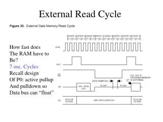
Defining the Read Cycle
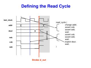
This document details the definitions and procedures for the Read and Write Cycles in digital clock signal testing. It outlines the specific steps for the read cycle, including changing the address, asserting control signals, waiting for data output, and verifying the output data. Similarly, it describes the write cycle process, highlighting changes to the address and data input, along with the assertion of control signals. These guidelines are crucial for effective testing and validation of digital clock components in embedded systems. ###

Defining the Read Cycle
E N D
Presentation Transcript
test_clock addr dout don’t care rwb csb oeb Defining the Read Cycle read_cycle ( change addr; assert csb; assert oeb; wait; assert csb; assert oeb; wait; expect dout; wait; ) Strobe d_out
test_clock addr din don’t care rwb csb oeb Defining the Write Cycle write_cycle ( change addr; change din; assert csb; assert rwb; assert oeb; wait; assert csb; assert rwb assert oeb; wait; )