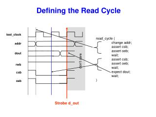
External Read Cycle
This article explores crucial concepts surrounding RAM speed, memory mapping, and the design considerations in embedded systems like the 8051 microcontroller. It discusses the implications of power supply noise on system stability, the necessary bypass capacitor sizes, and the impact of capacitive loads on performance. Key topics include address decoder logic for memory management, the importance of ensuring reliable data bus states, and practical strategies to mitigate voltage drops during rapid state changes. We'll also touch on networking and streaming challenges related to memory usage.

External Read Cycle
E N D
Presentation Transcript
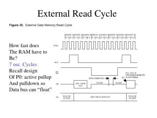
External Read Cycle How fast does The RAM have to Be? 7 osc. Cycles Recall design Of P0: active pullup And pulldown so Data bus can “float”
Memory Mapped System A[4:0] D[7:0] LCD \E3 ADC1 \E1 D[7:0] ADC2 \E2 D[7:0] PLD A[14:0] A[7:0] D[7:0] RAM \RE 32Kx8 \WE \E4 P0 P2 8051 ALE \RD \WD E LATCH D Q
Glue Logic Design • Define Memory Map • Ram: Upper 32K • LCD: 0-31 • ADC1: 32 • ADC2: 64 • Come up w/ address decoder logic for each case (many to 1 ok, 1 to many not okay!) • E4 = A15 covers only upper 32K addresses • E3 = A15’A6’A5’ covers 2^12 addresses including 0-31 but excluding upper 32K, 64, 32 • E2 = A15’A6’A5 covers 2^13 addresses but excludes upper 32K, 64, 0-31 • E1 = A15’A6A5’ covers 2^13 addresses but excludes upper 32K, 32, 0-31 • Account for inversions, and qualify with RD • \E4 = E4’ //RAM already qualified by \RE • \E3 = E3’+\RD • \E2 = E2’+\RD • \E1 = E1’+\RD
Power Supply Noise 8051 Why? power supply can’t change instantaneously Power lines have inductance Rapidly reduced Reff at constant I Voltage drop at the load So what? Could cause processor to reset/go to unknown state
What to do about it? 8051 Called a “Bypass Cap” How big should cap be? Depends on speed and inductance of the supply, and DI when switched Typical values for digital boards are .1uF/IC placed very close to IC ….then there’s capacitive loads….
Capacitive Loads chrg flash chrg flash chrg 8051 C1 C2 Why is this worse than resistive load? Recharge current is only limited by available electrons! Can cause massive voltage drop until battery catches up. So what? Last year’s capstone project: sonar firing caused processor reset
Charge Sharing V0 • Initially Q1=V0C1 • Then close switch, what is V’/V0 ? • V0 = Q1/C1 (initial condition) • Q1’+Q2’ = Q1 (post condition) • Q1 = V’C1+V’C2 = V’(C1+C2) • V’ = Q1/(C1+C2) • V’/V0 = Q1/(C1+C2) * C1/Q1 • V’/V0 = C1/(C1+C2) • If C1 dominates, then V’ ~ V0 • If C1 = 10C2 Then V1/V0 = 10/11 C1 C2
Other Business Streaming v. Local RAM Streaming Rate of consumption v. Need for buffering (Pilot/PC, 8051) Network Congestion RAM: Laziness Standalone Wiring Next Week’s Lab? Post Meeting Notes Rest of Class Schedule Major Topics: Embedded HW (Mostly Finished) Embedded OS (Next) Embedded Networking Software Engineering Concepts for Embedded/RT