FET ( Field Effect Transistor)
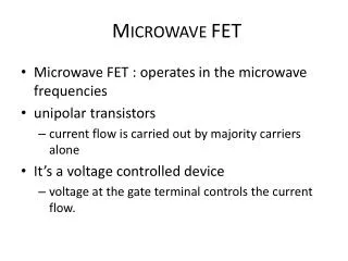
FET ( Field Effect Transistor). Few important advantages of FET over conventional Transistors. Unipolar device i. e. operation depends on only one type of charge carriers ( holes or electrons) Voltage controlled Device (gate voltage controls drain current)

FET ( Field Effect Transistor)
E N D
Presentation Transcript
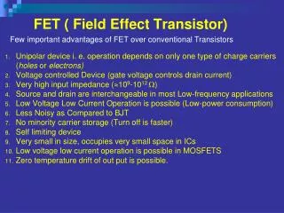
FET ( Field Effect Transistor) Few important advantages of FET over conventional Transistors Unipolar device i. e. operation depends on only one type of charge carriers (holes or electrons) Voltage controlled Device (gate voltage controls drain current) Very high input impedance (109-1012 ) Source and drain are interchangeable in most Low-frequency applications Low Voltage Low Current Operation is possible (Low-power consumption) Less Noisy as Compared to BJT No minority carrier storage (Turn off is faster) Self limiting device Very small in size, occupies very small space in ICs Low voltage low current operation is possible in MOSFETS Zero temperature drift of out put is possible.
Types of Field Effect Transistors (Classifications) n-Channel JFET p-Channel JFET FET Enhancement MOSFET Depletion MOSFET n-Channel DMOSFET p-Channel DMOSFET n-Channel EMOSFET p-Channel EMOSFET • JFET MOSFET (IGFET)
The Junction Field Effect Transistor (JFET) Figure: n-Channel JFET.
Drain Drain Drain Gate Gate Gate Source Source Source JFET SYMBOLS n-channel JFET p-channel JFET n-channel JFET (Offset-gate symbol)
Biasing the JFET Figure: n-Channel JFET and Biasing Circuit.
Operation of JFET at Various Gate Bias Potentials Figure: The nonconductive depletion region becomes broader with increased reverse bias. (Note: The two gate regions of each FET are connected to each other.)
Operation of a JFET Drain - N Gate P P + + - DC Voltage Source - N + Source
Simple Operation and Break down of n-Channel JFET Figure: n-Channel FET for vGS = 0.
N-Channel JFET Characteristics and Breakdown Break Down Region Figure: If vDG exceeds the breakdown voltage VB, drain current increases rapidly.
Transfer (Mutual) Characteristics of n-Channel JFET IDSS VGS (off)=VP Figure: Transfer (or Mutual) Characteristics of n-Channel JFET
Biasing Circuits used for JFET Fixed bias circuit Self bias circuit Potential Divider bias circuit
JFET (n-channel) Biasing Circuits For Fixed Bias Circuit Applying KVL to gate circuit we get and For Self Bias Circuit Where, Vp=VGS-off & IDSS is Short ckt. IDS
JFET Biasing Circuits Count… or Fixed Bias Ckt.
JFET Self (or Source) Bias Circuit This quadratic equation can be solved for VGS & IDS
V V DD DD R 1 D i i G R s + C i S i o + C + o v R 2 s v i _ R v R SS L o _ _ Common Drain (CD) Amplifier (also called “source follower”) FET Amplifier Configurations and Relationships: Note: The biasing circuit is the same for each amp.