Reverse Costing analysis
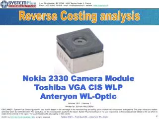
Reverse Costing analysis. 9 rue Alfred Kastler - BP 10748 - 44307 Nantes Cedex 3 - France Phone : +33 (0) 240 180 916 - email : info@systemplus.fr - website : www.systemplus.fr. Nokia 2330 Camera Module Toshiba VGA CIS WLP Anteryon WL- Optic. October 2011 - Version 1

Reverse Costing analysis
E N D
Presentation Transcript
Reverse Costinganalysis 9 rue Alfred Kastler - BP 10748 - 44307 Nantes Cedex 3 - FrancePhone : +33 (0) 240 180 916 - email : info@systemplus.fr - website : www.systemplus.fr Nokia 2330 Camera Module Toshiba VGA CIS WLP Anteryon WL-Optic October 2011 - Version 1 Written by: Sylvain HALLEREAU DISCLAIMER : System Plus Consulting provides cost studies based on its knowledge of the manufacturing and selling prices of electronic components and systems. The given values are realistic estimates which do not bind System Plus Consulting nor the manufacturers quoted in the report. System Plus Consulting is in no case responsible for the consequences related to the use which is made of the contents of this report. The quoted trademarks are property of their owners.
Table of Contents • Glossary • 1. Overview / Introduction……….……………….…........…4 • Executive Summary • Reverse Costing Methodology • 2. Companies Profile……………..……………….……....….6 • CMOS Image Sensors – Volume Shipments • Toshiba Profil • Anteryon Profil • 3. Nokia 2330 Teardown………………………….……....…12 • 4. Physical Analysis………………………...……….............16 • Synthesis of the Physical Analysis • Physical Analysis Methodology • Camera Module Views & Dimensions • Camera Module Disassembly • CIS Views & Dimensions • CIS Markings • CIS Bonding • CIS Microlenses • CIS Pixels • CIS Technology node • CIS Back view • Camera Module Cross-section • Package Cross-section • Optical Module Cross-section • CIS Packaging Cross-section • CIS Cross-section • Physical Data Summary • 5. Manufacturing Process Flow…….…………………..….64 • Global Overview • CIS Process Flow • CIS Wafer-level packaging Process Flow • Description of the CIS Wafer Fabrication Unit • WL-Optic Process Flow • Description of the WL-Optic Wafer Fabrication Unit • Final Assembly Process Flow • 6. Cost Analysis………………………….………………..…..79 • Synthesis of the Cost Analysis • Main Steps of Economic Analysis • Yields Explanation • Yields Hypotheses • CIS Front-End : Hypotheses • CIS FEOL + BEOL Cost • CIS Front-End Cost • CIS Back-End 0 : 1st Probe Test & Optical Test • CIS WLP Cost • CIS WLP Cost per Process Steps • CIS WLP : Equipment Cost per Family • CIS WLP : Material Cost per Family • CIS Die Cost • WL-Optic : Hypotheses • WL-Optic Front-End Cost • WL-Optic Cost per Process Steps • WL-Optic : Equipment Cost per Family • WL-Optic : Material Cost per Family • WL-Optic : Test, dicing and assembly • WL-Optic Price • Back-End : Final Packaging & Test • Camera Module Cost (CIS + WLO + Packaging) • 7. Estimated Price Analysis….………………….……..…..110 • Definition of Prices • Manufacturer Financial Ratios • Camera Module estimated Manufacturer Price
Physical Analysis Methodology • Package is analyzed and measured. • X-ray pictures are used to identify the package construction and the redistribution. • One cross-section is realized to get overall package data : dimensions, main characteristics. • An analysis of the technologies and of the materials used is performed. The schematic diagram below is constructed from observations made during this study and presented in the next slides. Polymer lense layer #1 Cap in glass fiber filled plastic SAMPLE Chrome AP layer Glass lense Lens plate glass wafer IR filter layer Glue Polymer lense layer #2 Bronze exterior part Glass spacer Polymer Convex lens layer #3 Glue Glass carrier Spacer wafer CIS photo-diodes TSV Silicone-epoxy glue Redistribution layer + bumps
Camera Module Disassembly SAMPLE
CIS Microlenses SAMPLE
Camera Module Cross-Section SAMPLE Camera module cross-section – SEM view
CIS Packaging Cross-Section SAMPLE
CIS Process Flow SAMPLE
CIS FEOL+BEOL Cost SAMPLE

