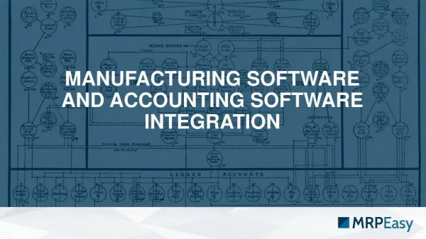
SOFTWARE INTEGRATION USING STEP AP210
SOFTWARE INTEGRATION USING STEP AP210. Prof. Jan Helge Bøhn Virginia Tech, Mechanical Engineering Blacksburg, Virginia 24061, USA Tel: +1-540-231-3276, Fax: +1-540-231-9100 E-mail: bohn@vt.edu, Mobile: +1-540-819-0326

SOFTWARE INTEGRATION USING STEP AP210
E N D
Presentation Transcript
SOFTWARE INTEGRATIONUSING STEP AP210 Prof. Jan Helge Bøhn Virginia Tech, Mechanical Engineering Blacksburg, Virginia 24061, USA Tel: +1-540-231-3276, Fax: +1-540-231-9100 E-mail: bohn@vt.edu, Mobile: +1-540-819-0326 NASA's STEP for Aerospace Workshop • January 16-19, 2001 • JPL, Pasadena, CA
CPES overview Why software integration? Sample demonstration case A first generation implementation Current activities STEP AP210 mini-consortium Presentation Outline NASA's STEP for Aerospace Workshop • January 16-19, 2001 • JPL, Pasadena, CA
National Science Foundation (NSF) Engineering Research Center (ERC) Five universities Virginia Tech, Univ. Wisconsin (Madison), RPI, NC A&T, Univ. Puerto Rico (Mayagüez) 85+ corporate members $120M budget over 10 years (year 3) CPES Overview NASA's STEP for Aerospace Workshop • January 16-19, 2001 • JPL, Pasadena, CA
Improve the competitiveness of US power electronics industry by developing an integrated systems approach via Integrated Power Electronics Modules (IPEMs) 10 x improvement in quality, reliability, and cost effectiveness of power electronics systems CPES Vision NASA's STEP for Aerospace Workshop • January 16-19, 2001 • JPL, Pasadena, CA
To achieve these goals, we must push existing technologies to their limits and develop new ones as needed use a multi-disciplinary set of software tools for design, modeling, and analysis, to optimize performance integrate our software tools Why Software Integration? NASA's STEP for Aerospace Workshop • January 16-19, 2001 • JPL, Pasadena, CA
The Multi-Disciplinary Analysis and Design Process Prototype 3D Solid-Body Modeling FE Stress & Strain Analysis FE Stress & Strain Analysis Cost Modeling Lumped Mechanical Parameter Extractor Mechanical Layout Geometry data Prototype Prototype FE Thermal Analysis FE Thermal Analysis Lumped Thermal Parameter Extractor Engineer Geometry data Lumped Electrical Parameter Extractor Circuit Diagram Multi- Disciplinary Lumped Parameter Simulator FE EM Field Analysis FE EM Field Analysis Electro- Dynamic Analysis Geometric Modeling Cost Modeling Engineer Electrical Circuit Simulation NASA's STEP for Aerospace Workshop • January 16-19, 2001 • JPL, Pasadena, CA
The CPES Solution Ever since CPES was first proposed in 1993: Software integration should rely on open international standards — and in particular STEP AP210 NASA's STEP for Aerospace Workshop • January 16-19, 2001 • JPL, Pasadena, CA
CPES Solution: Target Platforms 3D Solid Modeling I-DEAS Mechanical ABAQUS Cost Model and Analysis Data Flow AP 210 STEP Product Database Thermal FLOTHERM Program Flow Control iSIGHT Electro- Magnetic MAXWELL Reliability (CALCE) Electro- Dynamic SABER NASA's STEP for Aerospace Workshop • January 16-19, 2001 • JPL, Pasadena, CA
Sample Demonstration Case OBJECTIVE:Sample demonstration case to illustrate usefulness of integration of software tools for design, modeling, and analysis of an IPEM: • 3D solid modeling • Electrical modeling and analysis • Thermal modeling and analysis • Automated optimization • Experimental verification NASA's STEP for Aerospace Workshop • January 16-19, 2001 • JPL, Pasadena, CA
IPEM L1 P On-board S1 Converter Vin Lo L 3 V o Power O Factor Co S2 Correction L 2 N On-board Converter High Volt VRM Pre- regulator Low Volt VRM IPEM PCB Sample Demonstration Case DPS IPEM Design APEP Mechanical CAD IPEM: Two MOSFETs in a half-bridge structure as part of a front-end converter in a distributed power system (DPS). NASA's STEP for Aerospace Workshop • January 16-19, 2001 • JPL, Pasadena, CA
MOSFET Power Devices Aluminum Oxide (Al2O3) Solder Copper (Top & Bottom) Thermal Grease Heat Sink Sample Demonstration Case • The two MOSFETs are soldered on one side of a Al2O3 Direct Bonded Copper (DBC) board. • The copper substrate of the DBC is etched to give it the desired pattern. • Wire-bonding is used to connect the MOSFETs to the copper substrate. • The copper substrate on the other side of the DBC is attached directly to the heat sink. NASA's STEP for Aerospace Workshop • January 16-19, 2001 • JPL, Pasadena, CA
Parasitic Inductance Ideal Case S1 Vin Lo V o Co S2 Voltage waveform of the bottom switch at turn off Non-ideal Case S1 Vin Lo V o Co S2 Voltage waveform of the bottom switch at turn off To minimize the parasitic inductance, we want to place these two MOSFETs as close together as possible... NASA's STEP for Aerospace Workshop • January 16-19, 2001 • JPL, Pasadena, CA
Thermal Considerations But if we place these two MOSFETs too close together, then the thermal interaction between them may cause the junction temperature to become too high We therefore • Need electrical and thermal models that are based on 3D solid geometry to address these issues • Need to integrate the electrical and thermal analysis tools to quantify these effects NASA's STEP for Aerospace Workshop • January 16-19, 2001 • JPL, Pasadena, CA
Step 1 35mm 49mm P MOSFET N O Wirebond I-DEAS 3D Solid Model I-DEAS 3D Solid Model of the IPEM With I-DEAS we can describe all the necessary geometry and material information NASA's STEP for Aerospace Workshop • January 16-19, 2001 • JPL, Pasadena, CA
Step 2 P N O Maxwell Q3D Model (Parasitic Parameter Extraction) M13 M12 L1 M23 L2 L3 Parasitic Inductance Maxwell Q3D Model of the IPEM With Maxwell Q3D Extractor we can calculate the inductance from the geometry { using the partial element equivalent circuit (PEEC) method } NASA's STEP for Aerospace Workshop • January 16-19, 2001 • JPL, Pasadena, CA
Step 3 S1 P O P N N S2 S1 O S2 Maxwell Q3D Extractor Saber Model of the IPEM Saber Model (losses, EMI) With Saber we can determine losses and EMI { using the equivalent inductance matrix obtained from Maxwell } NASA's STEP for Aerospace Workshop • January 16-19, 2001 • JPL, Pasadena, CA
IPEM Maxwell Q3D Parameter Extractor L1 P P S1 N Vin O Lo L 3 V o O Co S2 L 2 N Saber Simulation Result Waveform Measurement Result Voltage waveform of the bottom switch at turn off Experimental Verification NASA's STEP for Aerospace Workshop • January 16-19, 2001 • JPL, Pasadena, CA
Step 4 FLOTHERM Model of the IPEM Thermal Modeling FLOTHERM uses computational fluid dynamics (CFD) to predict air flow and heat transfer in and around the electronic systems Air flow The thermal analysis is based on: • Device power loss provided by Saber • Geometry provided by I-DEAS • Boundary condition, such as air flow rate and ambient temperature NASA's STEP for Aerospace Workshop • January 16-19, 2001 • JPL, Pasadena, CA
Power Devices Aluminum Oxide Copper (top & bottom) Solder Thermal Grease DBC Heat Sink Rj-hs << Rhs-a Results: Thermal Modeling OBSERVATIONS: • The thermal resistance of the heat sink is much larger than that of any other package component • The heat sink size is determined by the device loss NASA's STEP for Aerospace Workshop • January 16-19, 2001 • JPL, Pasadena, CA
Results: IPEM Geometry Large-Sized IPEM Small-Sized IPEM L: 4~16nH L: 6~12nH • CASE STUDY: Reduce the size of the IPEM • Does not affect the parasitic inductance since both the length and width of the trace are reduced NASA's STEP for Aerospace Workshop • January 16-19, 2001 • JPL, Pasadena, CA
Large-Sized IPEM Small-Sized IPEM T: 37C T: 40C Results: IPEM Geometry • CASE STUDY: Reduce the size of the IPEM • Does not affect the power density since the size of heat sink is mainly determined by the power loss NASA's STEP for Aerospace Workshop • January 16-19, 2001 • JPL, Pasadena, CA
Sample Conclusions • To minimize the parasitic inductance of the layout, we should keep the width of the copper trace as large as possible, but minimize the length of the trace. • Scaling down the size of the IPEM may not increase the high power density, because the heat sink size is mainly determined by the power loss. NASA's STEP for Aerospace Workshop • January 16-19, 2001 • JPL, Pasadena, CA
A First Generation Implementation of IPEM Design, Modeling, and Analysis Software Tools Integration NASA's STEP for Aerospace Workshop • January 16-19, 2001 • JPL, Pasadena, CA
I-DEAS Geometry Change Heat Sink Size data and program flow control Geometry IPEM geometry in Maxwell: Maxwell Q3D iSIGHT L, C EMI Change Thickness Saber Temperature Distribution in IPEM and Heat Sink: Device Temperature Device Temperature loss I-DEAS Thermal Flow Controlled by iSIGHT NASA's STEP for Aerospace Workshop • January 16-19, 2001 • JPL, Pasadena, CA
iSIGHT flow control Software Tools iSIGHT data storage I-DEAS (geometry) Geometry External I-DEAS Design Variables Heat sink size Heat sink thickness Maxwell Q3D see notes below Parasitics: L, C Saber Temperatures Losses I-DEAS (thermal) EMI “Chicken & egg” iteration Data Flow and Storage NOTES: Currently the heat sink thickness is provided as an explicit variable to Maxwell in addition to the geometry (which currently is transmitted only once in the form of an .STL file). Because Maxwell ignores the relative positioning of parts within an .STL file, these parts must be manually repositioned within Maxwell; hence, the geometry is only transferred once and the variable thickness is provided explicitly as it changes from one iteration to another. In the future, when using AP203/AP210, the entire geometry will, for each iteration, be transmitted to Maxwell without the need for manual repositioning of parts or the explicit information of heat sink thickness. NASA's STEP for Aerospace Workshop • January 16-19, 2001 • JPL, Pasadena, CA
Heat Sink length 76 mm Heat Sink length 30 mm Temp (°C) Current (A) Temp (°C) Current (A) Thickness (mm) Vary the Heat Sink Thickness After several iterations driven by iSIGHT, we can examine the tradeoff between EMI and device temperature. NASA's STEP for Aerospace Workshop • January 16-19, 2001 • JPL, Pasadena, CA
MOTIVATION:Once a model is defined, it is practical to optimize via an automatically driven sequence of analysis-redesign iterations. NEED: We need to optimize our IPEMs in order to reach our 10x improvement targets. PROBLEM:Lack of implemented standards for data exchange between our software tools makes it impractical to set up such a model... Conclusions NASA's STEP for Aerospace Workshop • January 16-19, 2001 • JPL, Pasadena, CA
Examine how STEP AP210 can represent IPEM models What are the limitations? How can we work around them? What must be changed? Establish a STEP AP210 mini-consortium within CPES to drive the deployment of AP210 among MCAD and ECAD vendors Test case: 1kW DC/DC power conversion module for server and low-end telecommunication systems. Current Activities NASA's STEP for Aerospace Workshop • January 16-19, 2001 • JPL, Pasadena, CA
CPES STEP AP210 Team: Yingxiang Wu, MS ME / MS CPE Jonah Z. Chen, Ph.D. EE Li Ma, Ph.D. EE Christelle Gence, visiting scholar Prof. Jan Helge Bøhn, ME Prof. Dushan Boroyevich, EE Prof. Elaine Scott, ME Acknowledgements NASA's STEP for Aerospace Workshop • January 16-19, 2001 • JPL, Pasadena, CA
Acknowledgements This work was supported primary by the ERC Program of the National Science Foundation under Award Number EEC-9731677 NASA's STEP for Aerospace Workshop • January 16-19, 2001 • JPL, Pasadena, CA

