Download
1 / 18
180 likes | 231 Vues
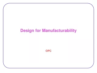
Design for Manufacturability. OPC. Sub-Wavelength Gap. Feature Size < Optical Wavelength. Limitations. Light diffraction phenomena in the sub-wavelength technologies major factors in yield rate Diffraction of light limits the critical dimension (CD),

E N D
Sub-Wavelength Gap • Feature Size < Optical Wavelength
Limitations • Light diffraction phenomena in the sub-wavelength technologies major factors in yield rate • Diffraction of light limits the critical dimension (CD), • such as the shortest length of the gate channel. • There are roughly 600 design rules for a typical 90 nm process. http://cc.ee.ntu.edu.tw/~ywchang/
Interference E at wafer
DSM Effects • Distortions: • corner rounding, • pulling back at the end of the narrow line, • wide variation of line width.
DSM Effects • Distortions: • corner rounding, • pulling back at the end of the narrow line, • wide variation of line width.
Solutions • Resolution Enhancement Technology (RET) • Optical Proximity Correction (OPC) • Phase-shifting Mask (PSM)
OPC Silicon Image w/o OPC Conventional (no OPC) • Corrective modifications to improve process control • As post-layout process • improve yield • improve device performance Original Layout 0.18 mm OPC Layout Silicon Image with OPC
OPC • OPC Features: • Serif • small L-shaped geometry added to (subtracted from) a convex (concave) corner to compensate for rounding • Hammerhead • a U or inverted-U geometry that compensates for line-end shortening • Scattering Bar (outrigger) • a disconnected, non-printing geometry that uses diffraction effects to enhance linewidth control • Notch • a local thinning of a feature to compensate for linewidth variation [Kahng, DAC99]
OPC-Friendly Routing • Problem: • the added feature narrows down the space between its neighbors. • Solution: • OPC-friendly routing • maximizes the effects of corrections and reduces the efforts that these fine features Li-Da Huang, Martin D. F. Wong, Optical Proximity Correction (OPC)-Friendly Maze Routing, DAC 2004
Original Layout Options by maze router
After OPC Process • Depending on the patterns and space between them, the features added by OPC can be quite complicated, • and they are considerably time-consuming.
Different Route for Elbow • The same three nets with different paths.
Less OPC Features Inserted • Fewer and less complicated OPC features are needed in the layout.
Reference • Minsik Cho, Joydeep Mitra, and David Z. Pan, “Manufacturability-Aware Routing ,” Handbook of Algorithms for Physical Automation, 2007.