Download
1 / 27
270 likes | 543 Vues
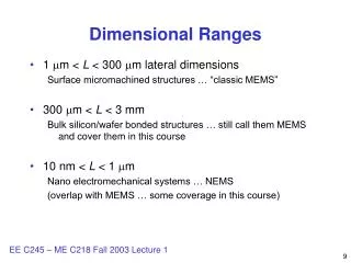
Dimensional Ranges. 1 m < L < 300 m lateral dimensions Surface micromachined structures … “classic MEMS” 300 m < L < 3 m m Bulk silicon/wafer bonded structures … still call them MEMS and cover them in this course 10 nm < L < 1 m Nano electromechanical systems … NEMS

E N D
Dimensional Ranges • 1 m < L < 300 m lateral dimensions Surface micromachined structures … “classic MEMS” • 300 m < L < 3 mm Bulk silicon/wafer bonded structures … still call them MEMS and cover them in this course • 10 nm < L < 1 m Nano electromechanical systems … NEMS (overlap with MEMS … some coverage in this course)
What aren’t MEMS • The Denso micro-car: circa 1991 http://www.globaldenso.com/ABOUT/history/ep_91.html • Fabrication process: micro electro-discharge machining It runs! Cost?
Experimental Catheter-type Micromachine for Repair in Narrow Complex Areas Japanese Micromachine Project 1991-2000
Batch Fabrication Technology • Planar integrated circuit technology 1958 - 1. Thin-film deposition and etching 2. Modification of the top few m of the substrate 3. Lateral dimensions defined by photolithography, a process derived from offset printing • Result: CMOS integrated circuits became the ultimate “enabling technology” by circa 1980 • Moore’s Law Density (and performance, broadly defined) of digital integrated circuits increases by a factor of two every year.
A Microfabricated Inertial Sensor MEMSIC (Andover, Mass.) Two-axis thermal-bubbleaccelerometer Technology: standard CMOS electronics with post processing to form thermally isolated sensor structures • Note: I’m a technical advisor to MEMSIC a spinoff from Analog Devices.
Other Batch Fabrication Processes • Historically, there aren’t that many examples outside of chemical processes • However, that’s changing: Soft (rubber-stamp) lithography Parallel assembly processes enable low-cost fabrication of MEMS from micro/nano components made using other batch processes … “heterogeneous integration”
Microassembly Processes Parallel Pick-and-Place Parallel assembly processes promise inexpensive, high-volume hetero-geneous integration of MEMS, CMOS, and photonics www.memspi.com, Chris Keller, Ph.D. MSE 1998 Fluidic Self-assembly Wafer-LevelBatchAssembly • Many challenges: • > interconnect > glue www.microassembly.comMichael Cohn, Ph.D. EECS, 1997 Uthara Srinivasan, Ph.D., Chem.Eng. 2001
A Brief History of MEMS:1. Feynmann’s Vision • Richard Feynmann, Caltech (Nobel Prize, Physics, 1965)American Physical Society Meeting, December 29, 1959: “What I want to talk about is the problem of manipulating and controlling things on a small scale. …. In the year 2000, when they look back at this age, they will wonder why it was not until the year 1960 that anybody began seriously to move in this direction.” “… And I want to offer another prize -- … $1,000 to the first guy who makes an operating electric motor---a rotating electric motor which can be controlled from the outside and, not counting the lead-in wires, is only 1/64 inch cube.” … he had to pay the electric motor prize only a year later • http://www.zyvex.com/nanotech/feynman.html
2. Planar IC Technology • 1958 Robert Noyce – Fairchild and Jack Kilby (Nobel Prize, Physics, 2000) -Texas Instruments invent the integrated circuit • By the early 1960s, it was generally recognized that this was the way to make electronics small … and cheaper Harvey Nathanson and William Newell, surface-micromachined resonant gate transistor, Westinghouse, 1965 Did Harvey hear about Richard Feynman’s talk in 1959? I don’t think so …
Why Didn’t MEMS Take Off in 1965? • Resonant gate transistor was a poor on-chip frequency reference metals have a high temperature sensitivity and don’t have a sharp resonance (low-Q) … specific application didn’t “fly” • In 1968, Robert Newcomb (Stanford, now Maryland) proposed and attempted to fabricate a surface micromachined electromagnetic motor after seeing the Westinghouse work Energy density scaling for this type of motor indicated performance degradation as dimensions were reduced … Materials incompatibility with Stanford’s Microelectronics Lab research focus on electronic devices became a major issue
Another Historical Current:Silicon Substrate (Bulk) Micromachining • 1950s: silicon anisotropic etchants (e.g., KOH) discovered at Bell Labs • Late 1960s: Honeywell and Philips commercialize piezoresistive pressure sensor utilizing a silicon membrane formed by anisotropic etching • 1960s-70s: research at Stanford on implanted silicon pressure sensors (Jim Meindl), neural probes, and a wafer-scale gas chromatograph (both Jim Angell) • 1980s: Kurt Petersen of IBM and ex-Stanford students Henry Allen, Jim Knutti, Steve Terry help initiate Silicon Valley “silicon microsensor and microstructures” industry • 1990s: silicon ink-jet print heads become a commodity
When the Time is Right … • Early 1980s: Berkeley and Wisconsin demonstrate polysilicon structural layers and oxide sacrificial layers … rebirth of surface micromachining • 1984: integration of polysilicon microstructures with NMOS electronics • 1987: Berkeley and Bell Labs demonstrate polysilicon surface micromechanisms; MEMS becomes the name in U.S.; Analog Devices begins accelerometer project • 1988: Berkeley demonstrates electrostatic micromotor, stimulating major interest in Europe, Japan, and U.S.; Berkeley demonstrates the electrostatic comb drive
Polysilicon Microstructures • UC Berkeley 1981-82 R. T. Howe and R. S. Muller, ECS Spring Mtg., May 1982
Polysilicon MEMS + NMOS Integration • UC Berkeley 1983-1984 Transresistance amplifier Capacitively driven and sensed 150 m-long polysilicon microbridge R. T. Howe and R. S. Muller, IEEE IEDM, San Francisco, December 1984
Polysilicon Electrostatic Micromotor Self-aligned pin-joint, madepossible by conformal depositionof structural and sacrificial layers Prof. Mehran Mehregany, Case Western Reserve Univ.
Electrostatic Comb-Drive Resonators • W. C. Tang and R. T. Howe, BSAC 1987-1988 New idea: structures move laterally to surface C. Nguyen and R. T. Howe, IEEE IEDM, Washington, D.C., December 1993
Analog Devices Accelerometers • Integration with BiMOS linear technology • Lateral structures with interdigitated parallel-plate • sense/feedback capacitors ADXL-05 (1995) Courtesy of Kevin Chau, Micromachined Products Division, Cambridge
Surface Micromachining Foundries 1. MCNC MUMPS technology (imported from Berkeley) 1992- 2. Sandia SUMMiT-IV and -V technologies: 1998 – 4 and 5 poly-Si level processes result: more universities, companies do MEMS M. S. Rodgers and J. Sniegowski, Transducers 99 (Sandia Natl. Labs)
Self-Assembly Processes • Alien Technologies, Gilroy, Calif. • chemically micromachined“nanoblock” silicon CMOS • chiplets fall into minimum energy • sites on substrate nanoblocks being fluidically self-assembed into embossed micro-pockets in plastic antenna substrate Prof. J. Stephen Smith, UC Berkeley EECS Dept.
More Recent History • Mechanical engineers move into MEMS, starting with Al Pisano in 1987 … expand applications and technology beyond EE’s chip-centric view • DARPA supports large projects at many US universities and labs (1994 – 200?) with a series of outstanding program managers (K. Gabriel, A. P. Pisano, W. C. Tang, C. T.-C. Nguyen, J. Evans) • Commercialization of inertial sensors (Analog Devices and Motorola polysilicon accelerometers 1991 → ) ≈ 108 by each company by 2002 • Microfluidics starts with capillary electrophoresis circa 1990; micro-total analysis system (-TAS) vision for diagnosis, sensing, and synthesis • Optical MEMS boom and bust: 1998 – 2002.
MEMS and Nanotechnology I • Richard Feynmann’s 1959 talk: “But it is interesting that it would be, in principle, possible (I think) for a physicist to synthesize any chemical substance that the chemist writes down. Give the orders and the physicist synthesizes it. How? Put the atoms down where the chemist says, and so you make the substance.” • Eric Drexler, 1980s: visionary promoting a molecular engineering technology based on “assemblers” … had paper at first MEMS workshop in 1987 • Early 1990s: U.S. MEMS community concerned that “far-out” nanotech would be confused with our field, undermining credibility with industry and government
MEMS and Nanotechnology II • Buckyballs, carbon nanotubes, nanowires, quantum dots, molecular motors, … together with the atomic-force microscope (AFM) as an experimental tool • Synthetic and “top-down” nanotechnology earns respect of MEMS community • Why is nanotechnology interesting? • Molecular control of sensing interface (chemical detection) • Synthetic processes promise to create new batch-fabrication technologies • Planar lithography is reaching into the nano regime (state-of-the are is 50 nm line/space; spacer lithography has reached 7 nm) • New computational devices: neural, quantum computing
1 GHz NEMS Resonator • Si double-ended tuning fork • tine width = 35nm • length = 500 nm • thickness = 50 nm • Interconnect parasitic elements are critical need nearby electronics • Uses vertical channel FINFET process on SOI substrate SOI Driveelectrode resonator SOI Senseelectrode L. Chang, S. Bhave, T.-J. King, and R. T. Howe UC Berkeley (unpublished)
MEMS (NEMS?) Memory: IBM’s Millipede Array of AFM tips write and read bits: potential for low and adaptive power
Electrostatic NEMS Motor Alex Zettl, UC Berkeley, Physics Dept., July 2003 multi-walled carbon nanotube rotary sleeve bearing 500 nm
Nanogap DNA Junctions • Development of ultrafast and ultrasensitive dielectric DNA detection • Applications to functional genomics or proteomics chips, as well as an exploration of nanogap DNA junction-based information storage and retrieval devices Luke P. Lee and Dorian Liepmann, BioEng. Jeff Bokor, EECS
Opportunities in Blurringthe MEMS/NEMS Boundary • Aggressive exploitation of extensions of “top-down” planar lithographic processes • Synthetic techniques create new materials and structures (nanowires, CNT bearings) • Self-assembly concepts will play a large role in combining the top-down and bottom-up technologies • Application: mainstream information technology with power consumption being the driver “Beyond CMOS” … really, extensions to CMOS > 2015 Non-volatile memories Communications