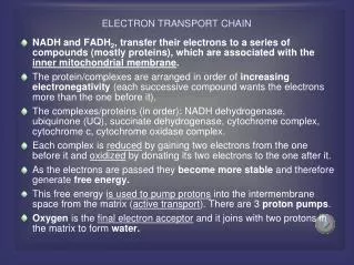
Download
1 / 22
250 likes | 469 Vues
Electron Transport of Metal Gated Devices in GaAs/AlGaAs Heterostructure. K. M. Liu( 劉凱銘 ) , W. R. Chen( 陳偉仁 ), Y. M. Lin ( 林玉敏 ), and S. Y. Hsu ( 許世英 ). Low Temperature Laboratory, Department of Electrophysics, National Chiao Tung University, Hsinchu, Taiwan, R.O.C. Outline. Introduction

E N D
Electron Transport of Metal Gated Devices in GaAs/AlGaAs Heterostructure K. M. Liu(劉凱銘) , W. R. Chen(陳偉仁), Y. M. Lin (林玉敏), and S. Y. Hsu (許世英) Low Temperature Laboratory, Department of Electrophysics, National Chiao Tung University, Hsinchu, Taiwan, R.O.C.
Outline • Introduction • GaAs/AlGaAs Heterostructure • Transport in mesoscopic system • Quantum Point Contact • Gate Defined Quantum Dot • Fabrication • Double quantum point contacts in series • Electron Pumping • Adiabatic Quantum Pumping • Summary
Structure of GaAs/AlGaAs grown by MBE 10 nm, GaAs Cap 8 nm, spacer AlGaAs 15 nm, δ- doping layer, Si, 2.6x1018 cm-2 0.2eV 60 nm, spacerAlGaAs, x=0.37 E1 2DEG 1500 nm, buffer layer GaAs Ec Ef 0.3mm GaAs substrate energy Introduction -GaAs/AlGaAs Heterostructure There is a very thin layer called 2-Dimensional Electron Gas(2DEG) at the interface of GaAs and AlGaAs. Which is a conducting layer. The mean free path is much larger than the limit length scale of modern technology. Thus we can obtain a system where the transport of electron is coherent and ballistic through lithographic fabrications.
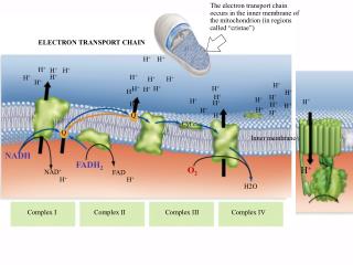
reservoir e- conductor T T μ1 R 1. Conductor with one channel -Landauer Formula 2. Multi-Channel Conductor Transport in Mesoscopic System –A Theoretical Description For an Ideal 1D system with one conducting channel In the limit of low temperature, small (μ1- μ2), and assume T(E) independent with E μ2 Current passing through a conductor can be expressed as v(k): electron velocity f(k): distribution function T(E): Transmission Transport is conductance!
e- Source Drain Vg E(kx) Ef kx Quantum Point Contact y x Applying a negative voltage on the metal split-gates fabricated above a 2DEG, depleting the electron gas, a quasi-1D quantum wire is formed. And the electron state in the conductor is quantized. Each plateau corresponds to an additional mode as integer multiples of half the Fermi wavelength.
- + Vg ΣC g R R l r dot C C l r - Vsd + Gate Defined Quantum Dot The modeled circuit: e- drain source 0.5μm The energy potential of QD can be tuned by varying Vg, and electron tunneling occurs when there is a state aligning with the Fermi level at source or drain. The energy is quantized as soon as the quasi-0Ddot is formed. And the transport is blocked as shown: Coulomb Blockade e2/Ceq charging energy μs N μD N+1 Vg
e- Coulomb Oscillation Coulomb Staircase Z. Phys. 85, 367(1991) PRL. 80, 4522(1998) For the I-V curve of the QD, the value of current corresponds to the number of states in the energy window Vsd and is quantized. 6-102a-I2 Weak Localization Number of electrons~1500
PR PR Coating & Prebake UV Light Exposure sample sample sample mask Hot plate 90°C Develop Fabrications Part I. Photolithography metal gates contact pads mesa
Electron Beam Exposure Coating & Prebake Develop (MIBK:IPA=1:3) electron beam PMMA sample PMMA sample sample Lift off in the Acetone metal Metal Deposition (Ti/Au) metal sample sample Part II. E-beam lithography
Double QPCs in Series (a)Vg2=-1V (b)Vg2=0V -J. Phys. C 21, L887 (1988) g1 g2 1 μm Channel length:0.3μm The second channel must impose a more severe constriction on the transverse momentum (Collimation) additional geometry resistance Remove the anomalous resistance As both QPCs are confined, the plateau index start from the smallest number among them the resistance through two QPCs isdetermined by the narrowest of the two constrictions.
Preliminary Summary e- Source V1 L V2 • Transport through single QPC demonstrates • quantized conductance in units of 2e2/h. • If the transport is ballistic, the total conductance across • double QPCs is determined by the smallest one. • The values are also integer multiples of 2e2/h. • It is theoretically predicted that: • When one of the QPC is in the tunneling regime (N<1), the transport should behave ohmic addition. qpc1 qpc2 Drain
Destruction of coherence in double quantum point contacts (QPCs) in series L=0.8μm • The traces have fewer plateaus with narrower qpc2. • It has only 1 plateaus with qpc2 set in N=2. It’s ballistic when L=0.8μm.
L=2.9μm • For larger L, subtracting the contribution from qpc2, • the single QPC’s conductance quantization is restored. • These two QPCs are almost independent with each other.
L=20μm • When the separation L is much larger than the mean free path, • identical traces were obtained. • These two QPCs are completely independent with each other.
As the transmission mode is set to zero (N<1) and L small, • we can regard qpc2 as a barrier, • and there’s no coherence between QPCs.Plateaus completely vanish.
Summary • Transport through double QPCs in series : • The transport behaviors are determined by two factors: • (a) separation between two QPCs, L. • (b) number of transmission modes N. • As L is larger than a specific length, order of e, • the transport behaves completely as that of • two independent QPCs. • As L is less than e and N is less than one , • the quantized conductance vanishes. • Coherence between QPCs can be destroyed.
Adiabatic Quantum Pumping PRB, 58, 10135(1998) X1 and X2 are two parameters modifying the wavefunction of the open dots. Which may be magnetic field or gate voltage. System: • Electron reservoirs are held at same voltage.(zero bias) • Each QPC have N channels at the Fermi level EF. • The scattering matrix of the system has dimension 2N×2N and is a function of X1 and X2 For two parameters X1 and X2 Small harmonic variation: Integrate over one period and use Green’s Theorem The charge δQ(m) entering or leaving the cavity through contact m(m=1,2) in an infinitesimal time: emissivity or
For a phase coherent quantum system, the out-of-phase variation will give rise to a dc current. • The current scales as the area enclosed by X1 and X2 in phase space or say the current varies as sinφ. Experiments: Science 283, 1905(1999) Isd=0
Pumped current in different dot size V Open dot qpc3 qpc4 Closed dot The pumped current reduces with increasing barrier height between dot and reservoirs.
Pumped current with different excitation amplitude • The pumped current enhances with increasing excitation amplitude. • Non-sinusoidal form when Vpp becomes too large.
Pumped current with different frequency The pumped current is roughly linear with frequency.
Summary • A mesoscopic system is easily achieved through GaAs/AlGaAs heterostructures due to it’s long mean free path. • The transport of electrons in such systems is characterized by transmission or conductance. • Quantum phenomenon: Quantized Conductance in QPC, periodic Coulomb Oscillations, Weak Localization. • Double QPCs in series is also studied, where the behavior is characterized by distance between QPCs. • Adiabatic Pumping can generate a DC voltage or current without external bias.