Download
1 / 18
180 likes | 432 Vues
MEMS 5-in-1 RM Slide Set #1. Reference Materials 8096 and 8097 The MEMS 5-in-1 Test Chips – Overview of the MEMS 5-in-1 RMs. Physical Measurement Laboratory Semiconductor and Dimensional Metrology Division Nanoscale Metrology Group MEMS Measurement Science and Standards Project.

E N D
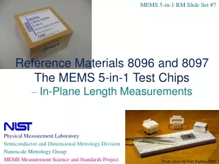
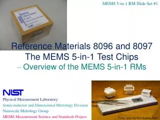
MEMS 5-in-1 RM Slide Set #1 Reference Materials 8096 and 8097 The MEMS 5-in-1 Test Chips – Overview of the MEMS 5-in-1 RMs Physical Measurement Laboratory Semiconductor and Dimensional Metrology Division Nanoscale Metrology Group MEMS Measurement Science and Standards Project Photo taken by Curt Suplee, NIST
Outline for the Overview of the MEMS 5-in-1 RMs
Why is MEMS Important? • A $10.2B industry (in 2011) • Yole forecasts $21.1B industry (in 2017) – doubled from 2011 • Growth rate (13 %/year) is healthy • MEMS being pulled into the market (esp. via the consumer market) • Spread out over many (say 100) smaller companies • MEMS acquisitions have soared in 2011 (>300 % increase) • MEMS is an enabling technology • Improved medical device performance • In-vitro diagnostics • Micro dispensers for drug delivery • Accelerometers in pacemakers • Wireless implants • Puts the “Smart” in Smart Phones • Accelerometers, gyros, pressure sensors, microphones,… • The future will see combination sensors • Etc. • As the field continues to grow, NIST can facilitate the introduction of product data sheets to allow inter-comparisons of consumer products. “MEMS Technology has the potential to change our daily lives as much as the computer has.” (Are we there yet?)
The MEMS 5-in-1 RM(What is it ?) MEMS = microelectromechanical systems 5-in-1 = test structures for five standard test methods on one physical test chip 1. Young’s modulus (SEMI MS4) 2. Residual strain (ASTM E 2245) 3. Strain gradient (ASTM E 2246) 4. Step height (SEMI MS2) 5. In-plane length (ASTM E 2244) RM = Reference Material: a material or substance one or more of whose property values are sufficiently homogeneous, stable, and well established to be used for the calibration of an apparatus, the assessment of a measurement method, or for assigning values to materials.
The 5 Standard Test Methods L These standards include precision and bias data (so considered validated standards) 1 ASTM E 2244 in-plane length SEMI MS2 step height 4 2 ASTM E 2245 residual strain SEMI MS4 Young’s modulus 5 ASTM E 2246 strain gradient 3 Calculations performed on the MEMS Calculator website (Standard Reference Database 166)
Uses of the MEMS 5-in-1 Photo taken by Curt Suplee, NIST • To validate use of the documentary standards (so companies can compare their in-house measurements taken on the RM with NIST measurements) • To characterize or validate a process • To take local measurements • To compare measurements meaningfully (e.g., between suppliers and customers) • To trouble-shoot a process (to improve yield and track failure sources to speed development) • To calibrate an instrument Intended for • MEMS designers • Test equipment manufacturers • Who may want to buy in bulk to sell with their instruments • IC and MEMS foundries and services
The 2 Types of Chips • RM 8097 • Fabricated using a polysilicon multi-user surface-micromachining MEMS process with a backside etch • Material properties of the first or second polysilicon layer are reported • Chip dimensions: 1 cm x 1 cm • RM 8096 • Fabricated on a multi-user 1.5 µm CMOS process followed by a bulk-micromachining etch • Material properties of the composite oxide layer are reported • Chip dimensions: 4600 µm x 4700 µm
NIST-on-a-Chip-type-of Packaging • testing solution provided • all measurements can be performed in this package chip lid PZT Photo taken by Erik Secula, NIST
The Chip Designs Each RM has 6 sections • Young’s modulus (uses SEMI standard MS4) • Residual strain (uses ASTM standard E 2245) • Strain gradient (uses ASTM standard E 2246) • Step height (uses SEMI standard MS2) • In-plane length (uses ASTM standard E 2244) • Certification Plus RM 8096 RM 8097
8 Properties Reported [using 5 Test Methods (TMs)] 1. Young’s modulus (uses SEMI standard MS4) 2. Residual strain (uses ASTM standard E 2245) 3. Strain gradient (uses ASTM standard E 2246) 4. Step height (uses SEMI standard MS2) 5. In-plane length (uses ASTM standard E 2244) 6. Residual stress (calculations in Young’s modulus TM SEMI MS4) 7. Stress gradient (calculations in Young’s modulus TM SEMI MS4) 8. Beam thickness a. For RM 8096 [uses step height TM (SEMI MS2) with electro-physical technique] b. For RM 8097 [uses step height TM (SEMI MS2) with opto-mechanical technique] 12
Example NIST Reference Values for RM 8096 Note: Effective values are reported if there are non-idealities associated with the geometry and/or composition of the test structures.
Material Available • NIST SP 260-177: A User’s Guide (2013 Edition) • The 5 standard test methods • Data analysis sheets • On the MEMS Calculator website (Standard Reference Database 166) • Accessible via the NIST Data Gateway (http://srdata.nist.gov/gateway/) with the keyword “MEMS Calculator” • Performs the calculations and verifies the data • Report of Investigation (ROI) • Includes NIST Reference Values: • A best estimate of the true value provided on a NIST Certificate/Certificate of Analysis/Report of Investigation where all known or suspected sources of bias have not been fully investigated by NIST
Instrumentation • Optical interferometric microscope (or comparable instrument) • In-plane length • Residual strain • Strain gradient • Step height • Thickness • RM 8096: When applicable platforms are reflective • RM 8097: For measurement of B and/or C (and perhaps A) • Optical vibrometer (or comparable instrument) • Young’s modulus • Stylus profilometer (or comparable instrument) • Thickness • RM 8096: When applicable platforms are not reflective • RM 8097: For measurement of A (for a lower uncertainty value), if used C
References • Overview articles 1. J. Cassard, J. Geist, and J. Kramar, “Reference Materials 8096 and 8096 – The Microelectromechanical Systems 5-in-1 Reference Materials: Homogeneous and Stable,” More-Than-Moore Issue of ECS Transactions, Vol. 61, May 2014. 2. J. Cassard, J. Geist, C. McGray, R. A. Allen, M. Afridi, B. Nablo, M. Gaitan, and D. G. Seiler, “The MEMS 5-in-1 Test Chips (Reference Materials 8096 and 8097),” Frontiers of Characterization and Metrology for Nanoelectronics: 2013, NIST, Gaithersburg, MD, March 25-28, 2013, pp. 179-182. 3. J. Cassard, J. Geist, M. Gaitan, and D. G. Seiler, “The MEMS 5-in-1 Reference Materials (RM 8096 and 8097),” Proceedings of the 2012 International Conference on Microelectronic Test Structures, ICMTS 2012, San Diego, CA, pp. 211-216, March 21, 2012. • User’s guide 4. J.M. Cassard, J. Geist, T.V. Vorburger, D.T. Read, M. Gaitan, and D.G. Seiler, “Standards Reference Materials: User’s Guide for RM 8096 and 8097: The MEMS 5-in-1, 2013 Edition,” NIST SP 260-177, February 2013 (http://dx.doi.org/10.6028/NIST.SP.260-177). • Standards 5. SEMI MS4-0212, “Test Method for Young’s Modulus Measurements of Thin, Reflecting Films Based on the Frequency of Beams in Resonance,” February 2012. (Visit http://www.semi.org for ordering information.) 6. SEMI MS2-0212, “Test Method for Step Height Measurements of Thin Films,” February 2012. (Visit http://www.semi.org for ordering information.) 7. ASTM E 2245-11, “Standard Test Method for Residual Strain Measurements of Thin, Reflecting Films Using an Optical Interferometer,” December 2011. (Visit http://www.astm.orgfor ordering information.) 8. ASTM E 2246-11, “Standard Test Method for Strain Gradient Measurements of Thin, Reflecting Films Using an Optical Interferometer,” January 2012. (Visit http://www.astm.org for ordering information.) 9. ASTM E 2244-11, “Standard Test Method for In-Plane Length Measurements of Thin, Reflecting Films Using an Optical Interferometer,” December 2011. (Visit http://www.astm.org for ordering information.) • Thickness articles 10. J.C. Marshall and P.T. Vernier, “Electro-physical technique for post-fabrication measurements of CMOS process layer thicknesses,” NIST J. Res., Vol. 112, No. 5, pp. 223-256, 2007. 11. J.C. Marshall, “New Optomechanical Technique for Measuring Layer Thickness in MEMS Processes,” J. of Microelectromechanical Systems, Vol. 10, No. 1, pp. 153-157, March 2001. • Fabrication 12. The RM 8096 chips were fabricated through MOSIS on the 1.5 µm On Semiconductor (formerly AMIS) CMOS process. The URL for the MOSIS website is http://www.mosis.com. The bulk-micromachining was performed at NIST. 13. The RM 8097 chips were fabricated at MEMSCAP using MUMPs-Plus! (PolyMUMPs with a backside etch). The URL for the MEMSCAP website is http://www.memscap.com.
Acknowledgment Mark Crockett (MEMSMART) Win Baylies (BayTech Group) • SEMI’s MEMS/NEMS Committee • MEMS Materials Characterization TF • ASTM’s E08 Committee on Fatigue and Fracture • E08.05 Subcommittee on Cyclic Deformation and Fatigue Crack Formation • E08.05.03 Task Group on Structural Films for MEMS • For industry cost-share and engineering support • MOSIS (for RM 8096) • MEMSCAP (for RM 8097) • NIST • Statistical Engineering Division, Measurement Services Division, Center for Nanoscale Science and Technology, Public and Business Affairs Office • Quality • Experts • MEMS Measurement Science and Standards Project • Test Structures Subgroup Sreeramesh Kalluri (Ohio Aerospace Institute) P. Thomas Vernier Busbee Hardy Robert Watters Stefan Leigh Ted Doiron Theodore Vorburger and David Read Craig McGray (Modern Microsystems) Yaqub Afridi (Potomac Networks) Brian Nablo Jon Geist (leader),Richard Allen