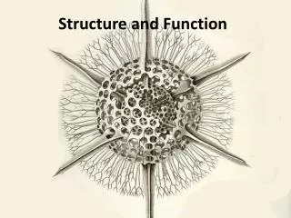
Structure/Function Relationships in Electronic Ceramics
Si(111). Si(111). Si(311). Si(311). flux at 10 keV. flux at 10 keV. 2.0x10 12 ph./sec. 2.0x10 12 ph./sec. 4.1x10 11 ph./sec. 4.1x10 11 ph./sec. flux at 20 keV. flux at 20 keV. 5.9x10 10 ph./sec. 5.9x10 10 ph./sec. 1.2x10 10 ph./sec. 1.2x10 10 ph./sec. spot size. spot size.

Structure/Function Relationships in Electronic Ceramics
E N D
Presentation Transcript
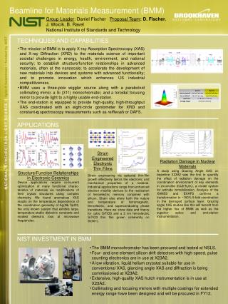
Si(111) Si(111) Si(311) Si(311) flux at 10 keV flux at 10 keV 2.0x10¹² ph./sec. 2.0x10¹² ph./sec. 4.1x10¹¹ ph./sec. 4.1x10¹¹ ph./sec. flux at 20 keV flux at 20 keV 5.9x10¹⁰ ph./sec. 5.9x10¹⁰ ph./sec. 1.2x10¹⁰ ph./sec. 1.2x10¹⁰ ph./sec. spot size spot size 0.18 mm x 0.18 mm 0.18 mm x 0.18 mm energy range energy range 4.5 keV to 25 keV 4.5 keV to 25 keV Beamline for Materials Measurement (BMM) Group Leader: Daniel Fischer Proposal Team: D. Fischer, J. Woicik, B. Ravel National Institute of Standards and Technology TECHNIQUES AND CAPABILITIES • The mission of BMM is to apply X-ray Absorption Spectroscopy (XAS) and X-ray Diffraction (XRD) to the materials science of important societal challenges in energy, health, environment, and national security; to establish structure/function relationships in advanced materials, often at the nanoscale; to accelerate the development of new materials into devices and systems with advanced functionality; and to promote innovation which enhances US industrial competitiveness. • BMM uses a three-pole wiggler source along with a paraboloid collimating mirror, a Si (311) monochromator, and a toroidal focusing mirror to provide light to a highly usable end-station. • The end-station is equipped to provide high-quality, high-throughput XAS coordinated with an eight-circle goniometer for XRD and constant-q spectroscopy measurements such as refflexafs or DAFS. APPLICATIONS Strain Engineered Electronic Thin Films Radiation Damage in Nuclear Materials A study using Grazing Angle XAS on beamline X23A2 was the first to quantify the effect of radiation damage on the coordination environment of key elements in zirconolite (CaZrTi2O7), a model system for actinide immobilization. Analysis of the XANES and EXAFS confirms a transformation to ~100% 5-fold coordination in the damaged surface layer. Grazing angle XAS studies like this will benefit from the higher flux of BMM as well as the superior optics and end-station instrumentation. Structure/Function Relationships in Electronic Ceramics Device applications require concurrent optimization of many functional characteristics of materials via modifications of their crystal structures using complex chemistry. We found anomalous XAS results on the temperature dependence of the coordination geometry of Ag(Nb,Ta)O3, the only known system that exhibits large, temperature-stable dielectric constants and modest dielectric loss at microwave frequencies. Strain engineering via epitaxial thin-film growth effectively tailors the electronic and mechanical properties of a material. Industrial applications range from enhanced electron mobility devices to the realization of ferroelectric memory conjoined with silicon. Strain also alters both the nature and temperature of ferromagnetic, ferroelectric, and superconducting phase transitions. Here we show data and theory for cubic SrTiO3 and a 2 nm ferroelectric SrTiO3 thin film grown coherently on Si(001). NIST INVESTMENT IN BMM • The BMM monochromator has been procured and tested at NSLS. • Four- and one-element silicon drift detectors with high-speed, pulse counting electronics are in use at X23A2. • A low vibration, liquid helium cryostat suitable for use in conventional XAS, glancing angle XAS and diffraction is being commissioned at X23A2. • Extensive, high-quality XAS hutch instrumentation is in use at X23A2. • Collimating and focusing mirrors with multiple coatings for extended energy range have been designed and will be procured in FY12.