Download

1 / 14
180 likes | 353 Vues
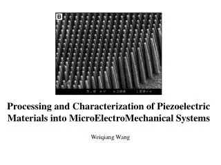
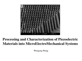
Processing and Characterization of Piezoelectric Materials into MicroElectroMechanical Systems. Weiqiang Wang. Outline. Introduction Lost silicon (Si) mold process for PZT ceramic microstructures PZT based piezoelectric micromachined switch Conclusion. Introduction.

E N D
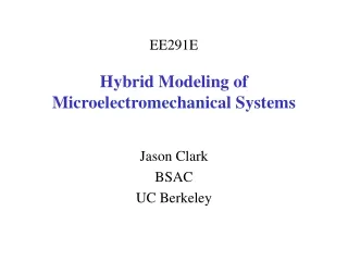
Processing and Characterization of Piezoelectric Materials into MicroElectroMechanical Systems Weiqiang Wang
Outline • Introduction • Lost silicon (Si) mold process for PZT ceramic microstructures • PZT based piezoelectric micromachined switch • Conclusion
Introduction MicroElectroMechanical Systems (MEMS) denote systems that include one or more small microstructures (sub- μm to mm) that often are fabricated using a technology μnamed micromachining, and materials,that originates partly from the semiconductor industry’s processes and partly from precision mechanics. • Piezoelectric effect direct piezoelectric effect converse piezoelectric effect Piezoelectric-based MEMS are generally attractive due to their high sensitivity and low electrical noise in sensing applications and high-force output in actuation applications • Exploiting the piezoelectric materials into microelectromechanical systems (MEMS) Lead zirconate titanate (Pb(ZrxTi1-x)O3, PZT) microstructures
Lost silicon (Si) mold process for PZT ceramic microstructures Fig. 1. Lost Si mold process
Results Fig. 2. SEM images of PZT microrods The PZT rods were 7 μm square in cross section with a 12 μm period. The resulting aspect ratio was more than 12.
Advantages • Fine scale and high aspect ratio. (rods 95 μm in diameter and 400 μm in height using lost plastic mold method. ) • Advantages of Si • high melting point (1440°C) and high strength • Si mold can be used as a part of the device • Si micromachining techniques have been well developed in-mold sintering Plastic mold: LIGA (lithography, galvanoforming, plastic molding) • HIP of PZT was successfully conducted at a temperature as • low as 800°C
Problems X-ray diffraction (XRD) analysesshows that perovskite PZT was the major phase, at the same time, certain amounts of undesired pyrochlore-type PZT phase was also observed. Oxygen deficiency But it is believed producing the same dense PZT rods at lower temperatures by increasing the HIPing pressures may suppress the formation of undesired phases.
Application 1-3 PZT/polymer composite piezoelectric transducers for medical imaging
PZT based piezoelectric micromachined switch Fig. 3. Schematic view of cantilever Fig. 4 Fabrication procedure Fig. 5 SEM of PZT deposited on substrate
Principle of operation Fig. 6 Schematic illustration of switch Fig. 7 SEM image of cantilever switch with transmission lines
Operation tests Low frequency test High frequency test Fig. 8 Switching response to a 1 Hz 20 V square wave Fig. 9 Switching response to (a) 30-V and (b) 50-V 2-μs pulse. Preliminary results using a gain-phase analyzer (HP4194A) have demonstrated that signals up to 100 MHz can be switched.
Discussion A one-degree-of-freedom dynamic model (1) k: spring constant; b=0 (2) : natural frequency; The time required to close the gap(δ) between the contact and the transmission lines can be obtained from (3) The calculated τon=3.3μs for this device, which is comparable to the measured value.
Conclusion Piezoelectric materials have been successfully applied in a variety of MEMS applications. The development of fabrication methods such as PZT structural micro-machining, low-stress silicon nitride deposition, and solution deposition of piezoelectric thin films has been essential. The MEMS applications described here compare favorably with other MEMS approaches based on commonly used electrostatic actuation. The continued promise for piezoelectric MEMS is attractive.
Click to edit company slogan . Thank You !