Development and Status of Eyelid Movement Sensor on Glasses: A Final Presentation
In this presentation by Danielle Perez and Shuki Eizner, under the guidance of Alexander Kinko, we cover the development of a portable and low-power Eyelid Movement Sensor Device (EMSD) that tracks eyelid movements through glasses. We discuss the project’s goals, design and activities, including the status of analog and digital PCB designs. The presentation also outlines the Gantt chart, next assignments, and detailed progress updates on the system's features such as data storage, battery management, and hardware testing.

Development and Status of Eyelid Movement Sensor on Glasses: A Final Presentation
E N D
Presentation Transcript
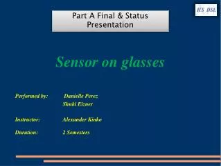
Sensor on glasses Part A Final & Status Presentation Performed by: Danielle Perez ShukiEizner Instructor: Alexander Kinko Duration: 2 Semesters
Table Of Contents • Short reminder -project’s goals. • project design. • Project activities and status . • Analogues PCB. • Digital PCB. • Next assignments. • Gantt chart.
Project’s Basic Concept Patient Doctor Eyelid Movement Sensor Device (EMSD) PC Application (Doctor’s workspace) Results of analysis
Project’s Goals Develop a portable, low-power system that will check the eyelid movements and analyzed the results. The system has the following features: • Portable system • Enables better tracking of the blinks by storing data, describing specific eyelid movement which include: • Starting and ending time (10-15 minutes each test) • Velocity • Frequency • Position • Have the ability to analyze each eye separately.
Project’s Goals – continue • Designing PCB, resulting in a small low-power eyelid movement sensor device (EMSD), which going to be placed on the glasses. • Powered by rechargeable battery, that is recharged by connection to the external power source. Low battery indicator alerts user when the battery is low.
Analogue PCB- activities and status • Preliminary design and characterization. • Found necessary HW for all features. • Electrical design. • Routing. • production. • Primary debug.
Routing Layer2-GND Layer1-TOP Layer4-Bottom Layer3-VDD
Digital PCB- activities and status • Preliminary design and characterization. • Found necessary HW for all features. • Electrical design for all possible hardware. • Routing. • Production.
Routing Layer1-TOP Layer2-VDD Layer4-Bottom Layer3-GND
Next assignments • HW debug which include the following tests: • LEDs – simple check that the LEDs are working, Check the intensity (in case of problems: • HW solution- Change the resistor value. • SW solution- PWM mechanism.) • Switches - simple check of controlling on other components by using the buttons. • Buzzer- check the buzzer by producing a voltage at 4kHz (needed: PWM mechanism)
Next assignments-cont’ • Crystals- check the correctness of the frequencies, the frequencies can be viewed using the scope. • EEPROM- write/read operation. (needed: relevant protocols, data organization) • Micro-SD- understanding and implementing the relevant protocol. write/read operation. (needed: relevant protocols, data organization) • USB- check the connectivity.
Next assignments-cont’ • Power module- LDO- checking the turning on/off mechanism DC2DC- check the conversion to 5V. (ENA=‘1’ => PG=‘1’) power manager- stat lines, the LEDs can reflect the battery stat, PM_BAT_STAT. (needed: A/D mechanism) • Connector- simple check with the scope to the analog waves, final check in the GUI interface. (needed: A/D mechanism, GUI interface)