CAD Tool Tutorial
CAD Tool Tutorial. Spring 2006 CSE598A / EE597G Analog-Digital Mixed-Signal CMOS Chip Design. NCSU CDK Environment Setup. Make your own Cadence project directory > mkdir ~userid/AMIS05 Copy setup files copy ‘copy’ file from ‘~chip/cadence/local/cdssetup’ to your project directory

CAD Tool Tutorial
E N D
Presentation Transcript
CAD Tool Tutorial Spring 2006 CSE598A / EE597G Analog-Digital Mixed-Signal CMOS Chip Design
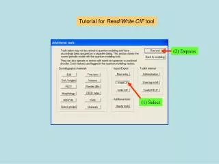
NCSU CDK Environment Setup • Make your own Cadence project directory > mkdir ~userid/AMIS05 • Copy setup files • copy ‘copy’ file from ‘~chip/cadence/local/cdssetup’ to your project directory > cp ~chip/cadence/local/cdssetup/copy . • run ‘copy’The setup files of NCXU CDK will be automatically copied to your project directory > copy
Running NCSU CDK • Source ‘cadence_env’ and execute ‘icfb’ > source cadence_env > icfb & • This will bring up a ‘CIW’ (Command Interpreter Window) and a ‘Library Manager’ Library Manager CIW
Creating a New Design • Create a new library in the Library Manager • File → New → Library…
Creating a New Design • In a ‘Create Library’ window • give a library name and a path where you want to create your library directory ex) Name: CSE598A Path: ~userid/AMIS05 • choose ‘Attach to existing tech library’ for ‘Technology Library’and select‘AMI 0.60u C5N(3M, 2P, high-res)’ • click ‘OK’
Creating a New Design • Now you have ‘CSE598A’ in a Library list • Create a ‘Cell View’ in your library • left click on your library ‘CSE598A’ in ‘Library Manager’ • File → New → Cell View… • in ‘Create New File’ windowput your ‘Cell Name’and select‘Composer - Schematic’for ‘Tool’ • click ‘OK’
Creating a New Design • Differential amplifier design • this is the schematic of the differential amplifier we’ll design Vdd M0 M1 OUT IN0 IN1 M2 M3 Vb M4 .
Schematic Design • Virtuoso Schematic Editor • design a schematic in this window • these are menu buttons on the left side Check and Save Property Save Instance Zoom in by 2 Wire (narrow) Zoom out by 2 Wire (wide) Stretch Wire Name Copy Pin Delete Cmd Options Undo Repeat
Schematic Design • Placing parts in the schematic • click ‘Instance’ button or type ‘i’ • in the ‘Component Browser’, select ‘NCSU_Analog_Parts’ and browse for the parts you need • you can changethe properties of the parts in‘Add Instance’
Schematic Design • Move • Edit → Move • Rotate / Sideways / Upside Down in ‘Move’ window • Wire • click ‘wire’ button or type ‘w’ • Changing property • select a part • click ‘property’ button or type ‘q’ • Zoom • click ‘Zoom’ button or select the area to zoom in with right mouse button
Schematic Design • Adding in/out pins • add a wire • click ‘Pin’ button or type ‘p’ • give a pin name andselect input/output • place a pin on a wire
Schematic Design • Check for any error • click ‘Check and Save’ button • make sure you don’tget warning or errormessage in CIW • Your design is nowready for a simulation
HSpice Simulation • Creating a netlist (1/4) • run ‘Analog Environment’ from ‘Schematic Editor’: Tools → Analog Environment
HSpice Simulation • Creating a netlist (2/4) • in the ‘Analog Environment’ window, setup a directory for simulation: Setup → Simulator/Directory/Host… • type in a directory name you want to create ex) ~userid/AMIS05/CSE598A/sim • click ‘OK’
HSpice Simulation • Creating a netlist (3/4) • in the ‘Analog Environment’ window, create a netlist: Simulation → Netlist → Create Final • the netlist will appear in a new window
HSpice Simulation • Creating a netlist (4/4) • save the netlist: File → Save as… • give a file name andclick ‘OK’
HSpice Simulation • Creating a Spice file (1/4) • running simulation (Spectre or Hspice) in Cadence is not set up yet • we need to create Spice file (.sp) manually for now • open the netlist at your terminal > nedit amp.net & • remove everything belowthe circuit netlist • modify the circuit netlist - AMI06N to nch - AMI06P to pch circuit netlist
HSpice Simulation • Creating a Spice file (2/4) • type in following Spice options .option post .option post_version=9007 .option ACCT=1 BRIEF=1 .option NUMDGT=8 MEASDGT=8 .option ACCURATE Spice options
HSpice Simulation • Creating a Spice file (3/4) • type in input sources VVDD! VDD! 0 3.3 VIN0 IN0 0 SIN 1.65V 0.5V 10x VIN1 IN1 0 1.65V VVB VB 0 1.15V input source
HSpice Simulation • Creating a Spice file (4/4) • type in the model library .LIB ‘/home/users2/kyusun/tool/model/libcmos050t22a.sp’ CMOS1 • type in an analysis type and .END .TRANS 0.01NS 500NS .END • save as amp.sp • refer to HSpice manuals for more information
HSpice Simulation • Running HSpice • source ~chip/.cad and execute HSpice > source ~chip/.cad > hsp amp • ‘AvanWaves’ will pop up when the simulation is done
HSpice Simulation • Simulation result • select an analysis type (Transient in this example) and double click the nodes to check the results • you’ll see display menus when right click on the display panel
Circuit Layout • Loading Virtuoso XL (1/2) • you are ready for a layout if your schematic meets a design specification • load ‘Virtuoso XL’ from the schematic editor Tools → Design Synthesis → Layout XL • select ‘Create New’and click ‘OK’
Circuit Layout • Loading Virtuoso XL (2/2) • select options in ‘Create New File’ - Library Name : CSE598A - Cell Name : amp - View Name : layout - Tool : Virtuoso • click ‘OK’
Circuit Layout • Virtuoso XL Layout Editor • layout your design in this window • these are menu buttons on the left side Save Undo Fit Edit Property Zoom in Instance Zoom out Path Stretch Polygon Copy Label Move Rectangle Delete Ruler
Circuit Layout • Generating transistors (1/2) • generate transistors and in/out pins from your schematic : Design → Gen From Source…
Circuit Layout • Generating transistors (2/2) • Layout Generation: I/O Pins, Instances • I/O Pins: select metal1/dg, set the size to 0.9x0.9, and click ‘Apply’ • click ‘OK’
Circuit Layout • Layout Editor (1/12) • tool generatedI/O pins andtransistors • we need to doplacing androuting • to see thetransistors,type ‘Shift+f’and to hide,type ‘Ctrl+f’ I/O pins transistors
Circuit Layout • Layout Editor (2/12) • click on a transistor in the layout editor • the corresponding transistor in the schematic editor will be highlighted
Circuit Layout • Layout Editor (3/12) • pins and instance names appear in the CIW when you click them in the layout editor
Circuit Layout • Layout Editor (4/12) • when you move an instance or an I/O pin, yellow lines will appear • these lines show where the ports or nodes need to be routed
Circuit Layout • Layout Editor (5/12) • LSW (Layer Selection Window) • user can select different layers ofthe mask layout • select a layer you want to editby clicking on the layer in LSWfor editing
Circuit Layout • Layout Editor (6/12) • there is a glitch in current layout editor setup • transistors are placed off-grid after generating layers in some case (this causes DRC errors) • to fix, go to ‘Display Options’- Options → Display… or type ‘e’ • change ‘Grid Controls’ - Type : Lines - Minor Spacing : 0.15 - Snap Spacing : 0 • click ‘OK’
Circuit Layout • Layout Editor (7/12) • move transistors and I/O pins to be placed on-grid • open ‘Display Options’ and go back to previous ‘Grid Controls’ (dots 1 5 0.15 0.15) on-grid off-grid
Circuit Layout • Layout Editor (8/12) • now place transistors as you want to layout • Rotate / Sideways / Upside Down are available in ‘Move’ window
Circuit Layout • Layout Editor (9/12) • perform DRC check often during layout design to prevent design rule violation • in layout editor : Verify → DRC… • click ‘OK’ • white markers indicateDRC errors
Circuit Layout • Layout Editor (10/12) • using ‘Ruler’ is helpful for resolving DRC errors, aligning cells, etc. • to create ruler: Window → Create Ruler or type ‘k’ • left click at a starting point and another left click at a final point • to clear all rulers : Window → Clear All Ruler or type ‘Shift+k’
Circuit Layout • Layout Editor (11/12) • routing - select a layer in LSW - click ‘Rectangle’ or type ‘r’ - draw a wire • contact - type ‘o’ - select contact type - number of contacts in row/column rectangle contact
Circuit Layout • Layout Editor (12/12) • run a final DRC checkwhen done with layoutand save your design
Netlist and Simulation • Netlist extraction (1/3) • run ‘Extractor’ - Verify → Extract…- click ‘Set Switches’- select ‘Extract_Parasitic_Caps’- click ‘OK’- check for any error message
Netlist and Simulation • Netlist extraction (2/3) • you may close layout editor and schematic editor windows now • double click ‘extracted’ view in your ‘Library Manager’ • a layout editor with the extracted view will pop up
Netlist and Simulation • Netlist extraction (3/3) • run ‘Analog Environment’ from ‘extracted view’: Tools → Analog Environment • following steps are same as simulating schematic design : refer to ‘Creating a netlist’, ‘Creating a Spice file’, and ‘Running HSpice’ [slides 13~21]
Product Documentation • Help • ‘HELP’ button in each window brings up product documentation • this is very useful for learning basic features ex) • or email jalim@cse.psu.edu documentation for ‘Stretch’ in layout editor

