Download

1 / 44
500 likes | 1.36k Vues
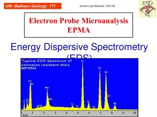
UW- Madison Geology 777. Version Last Revised: 2 /4/ 2014. Electron Probe Microanalysis EPMA. Energy Dispersive Spectrometry (EDS). UW- Madison Geology 777.

E N D
UW- Madison Geology 777 Version Last Revised: 2/4/2014 Electron Probe MicroanalysisEPMA Energy Dispersive Spectrometry (EDS)
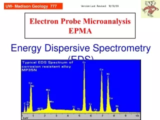
UW- Madison Geology 777 Using X-rays to produce e-hole pairs (charges proportional to X-ray intensity), which are amplified and then “digitized”, put in a histogram of number of X-rays counts (y axis) versus energy (x axis). A solid state technique with unique artifacts. What’s the point? EDS spectrum for NIST glass K309 (Goldstein et al, Fig. 6.12, p. 356)
UW- Madison Geology 777 Summary X-rays cause small electric pulses in a solid state detector. Associated electronics produce ‘instantaneously’ a spectrum, i.e. a histogram of counts (number=intensity) vs the energy of the X-ray Relatively inexpensive; there are probably 50-100 EDS detectors in the world for every 1 WDS (electron microprobe) Operator should be aware of the limitations of EDS, mainly the specific spectral artifacts, and the poor spectral resolution for some pairs of elements, and general lack of quality control of results
UW- Madison Geology 777 Electron gun Generic EMP/SEM Column/ Electron optics Optical microscope EDS detector Scanning coils SE,BSE detectors WDS spectrometers Vacuum pumps Faraday current measurement
UW- Madison Geology 777 Goldstein et al fig 5.21 EDS assemblage There are several types of solid state EDS detectors, the most common (cheapest) being the Si-Li detector. Components: thin window (Be, C, B); SiLi crystal, FET (field effect transistor: initial amp), cold finger, preamp, vacuum, amp and electronics (“single channel analyzer”).
UW- Madison Geology 777 Windows allow X-rays to pass and protect detector from light and oil/ice. Be: The most common EDS detector window has been made of Be foil ~7.6 mm (0.3 mil) thick. It allows good transmission of X-rays above ~ 1 keV. It is strong enough to withstand venting to atmospheric pressure, and opaque to optical photons. Thin - Ultrathin: For transmission of light element X-rays (<1 keV), windows ~0.25 mm thick of BN, SiN, diamond or polymer are used. They must use supporting grids to withstand pressure differentials; the grid (e.g., Si or Ni) takes up about 15% of the area, but the window material is thin enough that low energy X-rays pass through. EDS Windows This plots shows the transmittance of X-rays thru different types of window material. (Quantum [BN] 0.25 um, diamond 0.4 um). The higher the transmission number, the better “Windowless”: Here there is no film, and there is a turret that allows swapping with a Be window. Difficult to use as oil or ice can coat the detector surface. Not used much. Goldstein Fig. 5.41, p. 318
UW- Madison Geology 777 EDS Windows This plots shows the transmittance of X-rays thru different types of window material. (Quantum [BN] 0.25 um, diamond 0.4 um). The higher the transmission number, the better Goldstein Fig. 5.41, p. 318
A semi-conductor like Si has a fully occupied valence band and largely unfilled conduction band, separated by an energy gap (1.1 eV). Incident energy can raise electrons from the valence to the conduction band. How it works: energy gap X-ray hits the SiLi crystal, producing a specific number of electron-hole pairs proportional to X-ray energy; e.g. one pair for every 3.8* eV, so for incident Fe Ka, 6404 eV, 1685 e-hole pairs are produced. With a bias** applied across the crystal, the holes are swept to one side, the electrons to the other, producing a weak charge. Boron is important acceptor impurity in Si and degrades it (permits thermal excitation: bad); at the factory, Li is drifted in (donor impurity) to counter its effects. * 1.1 eV + energy wasted in lattice vibrations, etc Goldstein et al, Fig 5.19 **bias: a voltage is applied between 2 points; e.g. one +1500 v, other -1500 v.
For electronics, dope Si to change electronic structure: Si + Grp 5 (P, As) electrons majority carriers; Si + Grp 3 (B, Ga) holes majority carriers, BUT net effect is to allow current to flow in device in presence of bias – not good for an x-ray detector where you ONLY want current to flow when x-ray impacts. WANT HIGH PURITY Si (but Boron contaminant); so diffuse in Li (n-type dopant). Then drift with reverse bias. Result: Li-rich surface n-type; center: no-charge carriers (compensated); Low-Li p-type. Remove the ends. How they make the Si(Li) Williams 1987
UW- Madison Geology 777 How it works: inside the detector X-rays are absorbed by Si, with photoelectrons ejected. This photoelectron then creates electron-hole pairs as it scatters inelastically. The Si atom is unstable and will either emit a characteristic Auger electron or Si ka X-ray. If Auger, it scatters inelastically and produces electron-hole pairs. If Si Ka X-ray, it can be reabsorbed, in a similar process, or it can be scattered inelastically. In either case, the energy will end up as electron-hole pairs. The result, in sum, is the conversion of all the X-ray’s energy into electron-hole pairs -- with 2 exceptions. Fig 9.5 Reed; Fig 5.22 Goldstein
UW- Madison Geology 777 There are 2 exceptions to the neat explanation of how the Si(Li) detector works. Si-escape peaks are artifacts that occur in a small % of cases, where the Si ka X-ray generated in the capture of the original X-ray escapes out of the detector (red in figure). Since this X-ray removes 1.74 keV of energy, the signal generated (electron-hole pairs) by the incident X-ray will be 1.74 keV LOW. This will produce a small peak on the EDS spectrum 1.74 keV below the characteristic X-ray peak. Another artifact is the Si internal fluorescence peak, which occurs if an incident X-ray is absorbed in the Si “dead” layer (green Artifacts: Si-escape peak; Si internal fluorescence peak region). This region is “dead” to production of electron-hole pairs, but Si ka X-rays can be produced here which then end up in the “live” part of the detector, and result in a small Si ka EDS peak. Consider Ti … Fig 5.22 Goldstein et al
UW- Madison Geology 777 Artifacts: Si-escape peaks; Si internal fluorescence peak; extraneous peaks The figure shows a real spectrum of a sample of pure Ti metal -- but there are 7 peaks besides the Ti Ka and Kb. At 1.74 keV below each, are the respective escape peaks (blue arrows). Also present is a Si internal fluorescence peak (green arrow). The Fe and Cu peaks are from excitation of metal in chamber or sample holder by BSE or Ti X-rays. Note the sharp drop in the background intensity on the high side of the Ti Kb peak (= Ti K absorption edge, red arrow). (2 Ti Ka and Ti Ka+Kb explained shortly.) Note the scale of the spectrum: the Ti Ka max is 1.3 million counts. These effects are generally weak, but evident when you are looking for minor elements. Goldstein et al Fig 5.39,p. 316
UW- Madison Geology 777 Question: Do all characteristic X-rays have Si-escape peaks in a Si(Li) detector? Why or Why Not? Hint 1: Sr La does not, but Os Ma does Hint 2: Look up the characteristic energies of each Hint 3: Look up the absorption edge (critical excitation) energy of Si Ka Hint 4: Compare the numbers in 2 to number in 3. Which one is greater than the one in #3? Would a Si Ka x-ray produced in the sample, which then makes its way thru the vacuum to the EDS detector, have enough energy to knock out the inner shell (K) electron of the Si detector crystal?
UW- Madison Geology 777 Si(Li) detector has no internal gain*; for Ca Ka photon with ~1000 e-hole pairs, the charge is only ~10-16 Coulomb (weak!) Directly coupled to the Si crystal is a field effect transistor (FET) that converts charge to voltage, followed by a preamp. We need low noise, high gain amplification, so the Signal processing Si detector and FET are cooled to about 100K with liquid nitrogen (LN) to prevent noise (and prevent diffusion of Li in detector--at least in old ones). More signal gain provided by main amplifier (signal now boosted to 1-10 volts) where also RC (resistor-capacitor) circuits are used to shape the pulse, to maximize signal/noise ratio and minimize pulse overlap at high count rates. Then ADC (analog to digital converter) outputs data to the screen as a spectrum display. *gain = electronic multiplication of signal intensity
“ramp” UW- Madison Geology 777 The set of electron-hole pairs produced by the impact of the X-ray on the Si(Li) detector produces a tiny charge (~10-16 C), very quickly (~150x 10-9 sec). The FET(preamplifier) changes the charge (capacitance) into a tiny voltage (millivolts). These steps are shown in the first half of (a) to the right. The output of the FET is shown below at (b) where the x axis is time and y is voltage. The “jump” represents the presence of a voltage proportional to the number of electron-hole pairs generated by each X-ray, so Photon 2’s jump is of a higher energy than Photon 1’s jump which is higher than Photon 3’s jump. At a certain point the FET reaches the limit of the number of The first signals in the EDS detector charges it can hold, and then there is a reset or zeroing back to some baseline where it starts over. Following this are electronics to shape the voltage into a pulse that can be counted. Goldstein et al (1992), p. 297
UW- Madison Geology 777 Processing Time and Pulse Pileup Rejection The user can ‘tweak’ the time constant (T.C.) which sets the time allocated in the electronics to process each pulse (=X-ray). In the top figure, a short T.C. (1 ms) permits each pulse to be counted correctly. A longer T.C. (10 ms) means the “gate” is open longer and a second pulse can enter and be incorrectly added; this is “pileup” and causes distorted spectra. Therefore, circuits are added (#4, bottom figure) to sense when pileup occurs and to ignore that pulse. Goldstein et al (1992), Fig. 5.24 and 5.25, p. 300
40% 60% 80% Deadtiime UW- Madison Geology 777 “Deadtime” is the period during which the detector is “busy” and cannot accept/process pulses. This can introduce error unless it is accounted for, either by extending counting time, or correcting for it in the software. In most systems, the user sets the “live time” which is the time during which counts are actually counted, and the “real time” is automatically determined by the electronics or software. Optimal deadtime is in the 35-45% range. This optimizes both user/machine time and moderate to high throughput of counts. Dead Time Goldstein et al (1992), Fig. 5.25 (p. 300) and Goldstein et al (2003), Fig. 7.9 (p. 307)
UW- Madison Geology 777 The characteristic X-rays generated in the specimens are very close to lines, i.e. only a few eV wide at most. However, the conversion of X-ray to a pulse in the detector has several variables (imperfections) that broaden the peak to between maybe 135-200 eV, depending upon the type of detector and how well maintained it is. The narrowness of the peak is measured by the width of the peak at one half the maximum intensity of the peak -- this is what is termed the FWHM. Detector performance: peak resolution (FWHM) In EDS detectors, it is usually measured at the Mn Ka position, with values of 160 eV and below. Modern (2005) one are quoted at <130 eV. Goldstein et al, Fig 5.34, p. 311
UW- Madison Geology 777 Why Mn Ka for EDS resolution? EDS companies (their engineers mainly) do not want to have to carry around an SEM or EMP to be able to test, repair and calibrate an EDS system. Instead they carry a small 1” diameter x 2” long tube that fits over the end of the EDS “snout”. Inside it is an Fe-55 isotope source (half life 2.7 yr) which emits an intense x-ray at 5.985 keV which is only a few eV different than Mn Ka.
UW- Madison Geology 777 Time Constant+Beam Current--> Dead Time The above values are approximate, and meant only to show the relation of the variables.
UW- Madison Geology 777 The characteristic X-rays that we need to quantify “ride” atop the continuum, and the continuum contribution to the characteristic counts must be subtracted. (Top) Linear interpolation (B-D) will be in error due to the abrupt drop of continuum at the Cr K-absorption edge (5.989 keV). B-C is possible but critically dependent upon having good spectral resolution (<160 eV). A-B would be preferable. (Below) Doing background fit of a complex stainless steel. Spectral processing:background correction Goldstein et al Fig. 7.1,2, p. 367
UW- Madison Geology 777 Spectral processing:background modeling or filtering Correcting for the background is done by either of 2 methods: developing a physical model for the continuum, or using signal/noise filtering. Modeling is based upon Kramers Law: there is a function describing the continuum at each energy level, that is a function of mean atomic number, and measured “detector response”.
UW- Madison Geology 777 The spectrum of Kakanui hornblende (top left), with superimposed calculated (modeled) background, based upon Kramers Law*. Bottom figure shows after the background has been subtracted. Cu is artifact (stray X-rays). Mn is actually present at <700 ppm. Background Modeling Ij = constant x Z (E0 - Ej) / Ej at each energy channel j Goldstein et al Fig 7.4, p. 372
UW- Madison Geology 777 Theoretically Fourier analysis will separate out the low frequency continuum signal and high frequency ‘noise’ from the medium frequency characteristic peaks; however, there is overlap and the result is a poor fit. A better filter is the “top hat filter”, where no assumptions are made about the spectrum, and only the mathematical aspects of signal vs noise are considered. Background Filtering
UW- Madison Geology 777 This filter (top right) moves across the EDS spectrum (with an optimally defined window, ~ 2 FWHM* Mn Ka;~320 eV), and assigns a new value for the center channel based upon subtracting the values in the left and right channel from the center (value hk chosen to total area =0). Thus, in the simple spectrum (bottom right), the center channel (+), when the left and right channels are subtracted, leaves a value ~0. Top Hat Filtering *FWHM: full width at half maximum. Reed Fig 12.7 p. 174,Goldstein et al Fig 7.6, p. 374
UW- Madison Geology 777 More Artifacts: Sum Peaks true single X-ray peak, and includes it with all the other peaks from the elements actually present. For 2 major elements, could be 3 sum peaks; for 3, 6. In reality,you only see 1 or 2 unless you zoom in to the background level. Always consider their possible presence. There is a short period of time (t0) during each X-ray capture by the EDS detector, when the detector can capture a second X-ray “by mistake”. The electronics cannot distinguish this “sum peak” from a
UW- Madison Geology 777 …Fools even the pros Even the fanciest, slickest EDS setup can fool newcomers, not to mention experienced users. Above, is a partial spectrum (major peaks) of a commercial glass that has a lot of Si and O, plus Na and Al. Notice the S (Sulfur) label over a peak around 2.3 keV … sure looks like it might be Sulfur, right? It is NOT, rather it is a sum peak of O Ka (.525 keV)+ Si Ka (1.74 keV). Previous experience with this “fake” peak had taught me to be skeptical
UW- Madison Geology 777 In qualitative analysis of silicates, there are some combinations of element Ka peaks that fall close to Ka peaks of elements possibly present, as indicated in the table below: Sum Peaks Some of more advanced EDS software now contain algorithms to recognize and automatically remove sum peaks. But you must always be on guard for them, particularly ones which “could really be there”. In many of those cases, WDS is the solution.
UW- Madison Geology 777 There is always a potential for ‘stray’ X-rays being detected. It thus pays for the EDS operator to understand what the path is for the electron beam and for the X-rays, and know what ‘other’ elements might show up unintentionally. This is particularly true for EDS associated with TEM, where specimens routinely sit on grids (Cu?) and the high energy (200 keV?) electrons can go through the specimen and hit a metal part of column or chamber, with the resulting X-rays finding a way back to the detector. And More Artifacts
Family of Pd L lines UW- Madison Geology 777 Another thing: many SEM labs use gold or palladium coating on specimens. These very thin coats will produce definite x-ray peaks! And More Artifacts
UW- Madison Geology 777 …And beware of lazy peak IDs Even the fanciest, slickest EDS setup can make misidentifications…so the analyst cannot get lazy and assume just because the expensive software said something was there, it was there. I knew Arsenic was possible (As La identified), but unlikely, and rather Mg Ka was more likely. To confirm it was NOT As, I cranked the accelerating voltage up to 20 keV (the K shell binding energy is 11.9 keV) and found there was NO As Ka x-ray. Ergo, not As.
UW- Madison Geology 777 As Newbury (2005 and 2006 reply) pointed out, an EDS operator is a fool to believe that the automatic peak ID will be correct 99.9% of the time. …and trusting software From Newbury (2006)
UW- Madison Geology 777 Artifical EDS spectrum Artificial: no background, no artifacts, and assumes EACH element at 100% concentration. Why, then, the two slopes?? Peak intensities of elements from Si to Na decrease, and also from Si to Zn -- why? (Hint: 2 physical phenomena)
UW- Madison Geology 777 The actual spectrum of pure elements, as generated at the point of impact, would be one steady decreasing curve from Na down to Zn, following the red curve superimposed here. Artificial spectrum Slope down from Si to Zn: there are less and less X-rays being produced because the accelerating voltage is constant (e.g. 20 keV) and the overvoltage is lower. Slope down from Si to Na: X-ray energies are increasingly weaker, and are absorbed both within the specimen and by the window.
UW- Madison Geology 777 The spectrum on our monitor (d) is a result of many things impacting the real spectrum generated within the specimen (a). At instant of generation within the specimen, there is only the Ka, Kb and continuum. An instant later (b), as the X-rays leave the specimen, two things can happen: some of the continuum X-rays above 5.464 keV are absorbed, producing the drop in the continuum there. Evolution of EDS spectrum: from the specimen to the monitor - 1 Simulation of element (say V) X-ray generation and display Goldstein et al Fig 5.53 (by R. Bolon) p. 330
UW- Madison Geology 777 Also in (b) the lower energy continuum is absorbed, causing the dropoff in the spectrum there. When the X-rays hit the detector (c), Si fluorescence peaks can result. And after signal processing (d), the display will show peak broadening, sum peaks, Si-escape peaks, further decrease of intensity and low energy noise. Evolution of EDS spectrum: from the specimen to the monitor - 2 Simulation of element (say V) X-ray generation and display Goldstein et al Fig 5.53 (by R. Bolon) p. 330
UW- Madison Geology 777 That big tank of liquid nitrogen cools the SiLi crystal and the FET, so the very low charge generated by the electrons-holes can be detected with minimal noise. But what about letting the thing warm up when you’re on vacation? There is a lot of misunderstanding about this… Modern systems “can” be allowed to warm up without damage to the crystal (if the bias on it is turned off) -- BUT that is not the only thing to be concerned about when it warms up. Another important ingredient is the Comments about LN2 and EDS vacuum within the snout that extends from the bottom of the dewar to the end where the detector sits -- there is a “getter” (zeolites or Al wool) inside that absorb yucky contaminants. But if the getter warms up, they are released inside the snout, creating a poor vacuum, which then means the LN usage increases significantly as the vacuum is poor. Bottom line: keep it cold all the time.
UW- Madison Geology 777 EDS-WDS comparison
UW- Madison Geology 777 Over the past 15-20 years, 2 new “spins” off the ‘old school’ Si(Li) EDS detector have entered the microanalysis world: The microcalorimeter The Silicon Drift Detector Recent Developments
UW- Madison Geology 777 Microcalorimeter The principal behind the microcalorimeter is that an x-ray hitting a very sensitive thermal absorber will register a very small temperature increase. However, this requires a very cold absorber, with liquid helium cooling required. It would provide the best of both EDS and WDS, with simultaneous capture of all x-ray energies AND with very tight spectral resolution (like with WDS). However, there apparently have been major engineering stumbling blocks and none have made it to the market.
UW- Madison Geology 777 The SDD is similar to SiLi Detector in that electron-hole pairs are generated, but the physical design is radically different. There is a lower capacitance, and also a lower leakage current (high leakage current in SiLi is what requires LN cooling). And because the SDD has the FET “built in”, created during the lithography of the Si crystal, wires are eliminated, reducing capacitance more. Resulting advantages: Silicon Drift Detector LN not needed (use a simple Peltier cooler) Can handle high count rates >100,000 up to ~106 cps Spectral resolution at 100,000 cps still good (~140-150 eV)
Image from Bruker web page The SDD is created from a single Si crystal using micro-lithography. “The major distinguishing feature of an SDD is the transversal field generated by a series of ring electrodes that causes charge carriers to 'drift' to a small collection electrode. The 'drift' concept of the SDD (which was imported from particle physics) allows significantly higher count rates.” - Wikipedia
Silicon Drift Detector Simulation For the full simulation, go to http://www.ketek.net/products/sdd-technology/working-principle/ url updated 2/3/14
UW- Madison Geology 777 There are several modern EDS companies, with most producing very informative brochures that go into the technical details of EDS hardware (and software): For example: Oxford Instruments http://www.oxford-instruments.com/products/microanalysis/energy-dispersive-x-ray-systems-eds-edx/eds-for-sem/sdd has a nice technical publication explaining EDS using the SDD as the detector. Well worth downloading and reading. Further EDS details url updated 2/4/14