Download
1 / 30
310 likes | 542 Vues
EEE598 Molecular Electronics. Some Information about the Course. Instructor: Dr. Nongjian Tao ( njtao@asu.edu ) Where: ECA 219 When: TTH 12:00 – 1:15 pm Office Hours: TTH 1:30 - 2:30 p.m. or by appointment. Office Location: GWC 618

E N D
Some Information about the Course • Instructor: Dr. Nongjian Tao (njtao@asu.edu) • Where:ECA 219 • When:TTH 12:00 – 1:15 pm • Office Hours: TTH 1:30 - 2:30 p.m. or by appointment. • Office Location: GWC 618 Class Website: http://www.public.asu.edu/~ntao1/Teaching/EEE598/EEE598web2008.htm
Prerequisites • Basic quantum physics (e.g., EEE434) • General chemistry • Solid state electronics (e.g. EEE436)
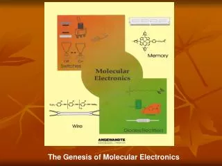
Course Objectives • Introduction to the frontiers in molecular electronics • Interdisciplinary approaches • Fundamental aspects of molecular electronics
TextbooksThere is no prescribed textbook for the course, but reference books and materials are listed below: • "Quantum chemistry", Ira N. Levine, Allyn and Bacon, 1970. • "The Chemical Bond", J.N. Murrell, S.F.A. Kettle and J.M. Tedder, John Wiley & Sons, 1987. • "Superamolecular Chemistry", J. W. Steed and J.L. Atwood, John Wiley & Sons, 2000. • "Designing the Molecular World", P. Ball, Princeton University Press, 1994. • "Introduction to Solid-State Physics", C. Kittle, John Wiley & Sons, 1986. • "Introduction to Mesoscopic Physics", Y. Imry, Oxford University press, 1997. • "Transport in Nanostructures", D.K. Ferry and S.M. Goodnick, Cambridge University Press, 1997. • "Intermolecular Surface Forces", J. Israelachvili, Academic Press, 1991.
Grading • Homework: 10% • Quiz I, II and III: 60% • Final Exam (term paper + Presentation): 30% • Homework Assignments • Homework assignments will usually be given in class and posted also on the class web page.
Materials to be Covered • Introduction • Molecular Electronics States • Electron Transport in Molecules • Molecular Devices • Special Topics
1. Introduction • What is molecular electronics? • Why molecular electronics? • Why now? • When are we going to have it?
Introduction • Feynman’s Talk in 1959: “There is Plenty of Room at the Bottom” http://www.zyvex.com/nanotech/feynman.html “What I want to talk about is the problem of manipulating and controlling things on a small scale.”
“Why cannot we write the entire 24 volumes of the Encyclopedia Brittanica on the head of a pin?” – Mass Storage Device. - each dot is about 10 nm wide, 1000 atoms. - DNA uses 50 atoms for a bit. - STM can use a single atom! (IBM) • “I don't know how to do this on a small scale in a practical way, but I do know that computing machines are very large; they fill rooms. Why can't we make them very small?! “ Miniaturizing computers
“What are the possibilities of small but movable machines? “ – Nanoelectromachanical Systems • “How do we make such a tiny machine? I leave that to you.” - It is MOLECULAR ELECRONICS!?
Acceptor Donor
Why Molecular Electronics? Semiconductor devices shrink to the nano-scale Transistor Size Year • If current trend continues, it will reach molecular scale in • two decades. • There are many molecules with interesting electronic properties.
Single-Electron Memory Cell e- Au Heme group e- Fe+3 Fe+2
Molecular Abacus The “bead” can be reversibly switched between two positions by pH. Ashton et al. JACS, 120, 11932(1998)
Molecular Motor Molecular Oscillator Angew. Chem., Int. Ed. 2000, 39, 3284-3287.
+ + + + K K Ag Ag Molecular Sensor Molecular Recognition: A capability that Si lacks Crown ether • A small difference in the diameters of the K+ and Ag+ • can cause a huge difference in the binding capacity
Homework 1.1). Read Feynman’s Talk in 1959: “There is Plenty of Room at the Bottom”. 1.2). To write the entire 24 volumes of the Encyclopedia Brittanica on the head of a pin, how small each bit has to be? 1.3) Read Angew. Chem., Int. Ed. 2000, 39, 3284-3287. Note: Exams will cover materials in your reading assignments!
What is Next Molecular Electronics States or Energy Diagram!
0 V Vg Vd > 0 METAL GATE OXIDE LAYER p+ orn+ Si p+ orn+ Si n- or p-TYPE Si 0 V Review: The MOSFET • The pn junction we have studied so far is a TWO TERMINAL device in which current flow is regulated by applying a voltage across the source and drain * Many semiconductor devices are THREE-TERMINAL structures however in which the current flow between source and drain is regulated by varying the voltage applied to a control GATE * An example of such a device is the METAL-OXIDE-SEMICONDUCTOR FIELD-EFFECT TRANSISTOR (MOSFET) a schematic diagram of which is shown below • A schematic illustration of the MOSFET • The substrate may be either p-type or n-type but thecontacts must be made of oppositely doped material • the MOSFET therefore looks like two pn junctionsthat are connected back-to-back • unless stated otherwise we will always assume thatthe source (left contact) is grounded while the drain(right contact) is positively biased with a voltage vd
VACUUMLEVEL Ec EF Ev Energy-Band Structure of the MOSFET • In order to understand the operation of the MOSFET we need to consider the details of its ENERGY-BAND structure * Shown below are the energy levels of the different components of the MOSFET and the resulting band structure of the final device For simplicity we assume that the workfunction of the metal and semiconductor are initially the SAME and that the semiconductor is n-type We also treat the insulating oxide layer as a WIDE-GAP semiconductor VACUUMLEVEL Ec Fm Fs Ec EF EF Ev Ev METAL OXIDE SEMICONDUCTOR MOSFET BAND STRUCTURE (vertical lines denote material surfaces)
Ec Ec EF EF Vg = 0 Vg > 0 Ei Ei Ev Ev • Application of a positive gate voltage LOWERS the Fermi level in the metal but leaves that in the semiconductor UNAFFECTED since NO current flows across the MOS boundary * The positive gate voltage therefore causes the energy bands of the semiconductor and the insulating layer to bend DOWNWARDS as the metal is approached Note that the band bending in the oxide layer varies LINEARLY as a function of position since there is assumed to be NO charge present in this layer
Vg < 0 Ec EF Ec Vg > 0 EF Ei Ei Ev Ev • The band-bending diagram clearly illustrates that with a positive voltage applied to the gate the electron concentration in the semiconductor is ENHANCED near the oxide interface * The Fermi level lies CLOSER to the conduction band near the interface and the positive gate voltage is said to cause ACCUMULATION since it increases the MAJORITY carrier concentration near the interface * Similar arguments show that a NEGATIVE gate voltages RAISES the Fermi level in the metal causing the energy bands in the oxide and semiconductor to bend UPWARDS Now the gate voltage causes DEPLETION of majority carriers at the interface ACCUMULATION MODE DEPLETION MODE
Ec EF EI Ev • An effect known as INVERSION occurs when the negative voltage applied to the gate is increased sufficiently * Eventually the Fermi level will lie closer to the VALENCE band at the interface and theHOLE concentration at this surface will exceed the electron concentration! In such a situation we have INVERTED the majority carriers at the interface * The CROSSOVER from depletion to inversion occurs once the Fermi level in the semiconductor DROPS BELOW the intrinsic Fermi level • energy band bending in the n-type semiconductor of a MOS capacitor with a large negative voltage applied tothe metal gate • at the point xo the equilibrium Fermi level in thesemiconductor coincides with the intrinsic Fermi level • for values of x greater than xo the Fermi level lies closerto the conduction band and the majority carriers areelectrons • for values of x less than xo the Fermi level lies closer tothe valence band and the majority carriers are holes • for values of x less than xo the semiconductor is thusinverted xo x
0 V Vg Vd = 0 METAL GATE OXIDE LAYER n+ Si n+ Si p-TYPE Si Ec EF Ev 0 V n-TYPE p-TYPE n-TYPE MOSFET Operation • To illustrate the principles of MOSFET operation we now consider the case of a structure formed on a p-TYPE substrate * Below we show the energy-band structure of the MOSFET in the case where NO voltage is applied to its gate This structure is easily drawn by realizing that the MOSFET LOOKS like twoBACK-TO-BACK pn junctions Note from this band diagram that an energy BARRIER exists that BLOCKS electron flow between the two n+ contacts
Ec EF Ev n-TYPE p-TYPE n-TYPE • With a POSITIVE voltage applied to the gate ELECTRONS are induced underneath it and a continuous CHANNEL eventually forms between the n+ contacts * Equivalently we may imagine that the gate voltage LOWERS the energy barrier to current flow This occurs once the gate voltage exceeds some THRESHOLD value VT • the figure left shows the energy bands of a p-type MOSFETwhen a positive voltage is applied to the gate • the energy barrier to diffusion is lowered allowing fora flow of current between the n-type contacts • this is said to be an example of an enhancement-mode MOSFETsince a gate voltage is required to induce the formation ofan electron channel underneath the gate • other types of devices known as depletion-mode MOSFETSalready have a continuous channel at zero gate voltageand the gate is then used to turn off the flow of currentthrough the device
0 V Vg Vd = 0 0 V Vg Vd > 0 METAL GATE METAL GATE OXIDE LAYER n+ Si n+ Si OXIDE LAYER n+ Si n+ Si p-TYPE Si p-TYPE Si • The current flowing through the MOSFET also depends on the value of the DRAIN VOLTAGE * Begin by considering a MOSFET in which the drain potential is set to zero and for which the gate voltage EQUALS the threshold value VT In this case a UNIFORM channel is formed between the n-type contacts * With a POSITIVE drain voltage applied however the voltage drop between the gate and the channel reduces from VT near the source to VT - Vd near the drain The channel therefore PINCHES OFF in the region near the drain
Id LINEAR SATURATED 0 V Vg Vd > 0 METAL GATE OXIDE LAYER n+ Si n+ Si Vd p-TYPE Si • The current flowing through the MOSFET therefore exhibits different behavior as we vary the DRAIN voltage * For SMALL drain voltages the current increases LINEARLY with drain voltage since the electron channel between the contacts remains CONTINUOUS * As the drain voltage is increased however the current eventually SATURATES as the channel pinches offThe current in this regime is carried by electrons that are pulled into the pinch-off region and travel at the co-called SATURATION drift velocity because of the HIGH electric field that exists along the channel Vg > VT Variation of channel current as a function of drain voltage in a typical mosfet
INCREASING Vg 0 V Vg Vd = 0 Id METAL GATE OXIDE LAYER n+ Si n+ Si INCREASING Vg Vd • As the gate voltage is INCREASED beyond the threshold for formation of the electron channel the current flowing at any given drain voltages also INCREASES * This is since the MOSFET may be considered as a variable resistor whose resistance is tuned by means of the gate voltage * As the gate voltage is increased the value of the drain voltage for which the saturation occurs also INCREASES Since a more positive drain voltage is required to pinch off the THICKER electron channel Increasing the gate voltage beyond thresholdcreates a thicker electron channel … … Consequently the channel pinches off ata higher drain voltage