Download
1 / 40
400 likes | 602 Vues
Molecular electronics by the Numbers. Sokrates T. Pantelides, Massimiliano Di Ventra, Norton D. Lang and Sergey N. Rashkeev. IEEE TRANSACTIONS ON NANOTECHNOLOGY, VOL. 1, NO. 1, MARCH 2002.

E N D
Molecular electronicsby the Numbers Sokrates T. Pantelides, Massimiliano Di Ventra, Norton D. Lang and Sergey N. Rashkeev IEEE TRANSACTIONS ON NANOTECHNOLOGY, VOL. 1, NO. 1, MARCH 2002
Molecular electronics by the NumbersSokrates T. Pantelides, Massimiliano Di Ventra, Norton D. Lang and Sergey N. Rashkeev • Molecules for nanoscale electronics device. • Experimentalmeasurements rich structure and diverse behavior. • I-V characteristiccomputed understanding of transport in molecules. • Informations obtained: molecule-electrode contacts; three-terminal molecular device; factors that control the performance.
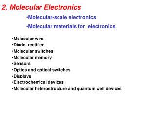
Molecular electronics by the Numbers • Introduction • Transport in a Single Benzene Ring • Three-Terminal Device • Benzene Ring With a Ligand • Conclusion
Molecular electronics by the Numbers • Introduction • Transport in a Single Benzene Ring • Three-Terminal Device • Benzene Ring With a Ligand • Conclusion
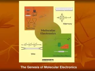
Transistors per chip 109 108 Pentium Pro 80786 107 80486 Pentium 106 80386 80286 105 8086 104 8080 4004 103 1970 1980 1985 1990 1995 2000 2005 2010 1975 Year Introduction The solid-state and silicon-based technology follows the Moore’s Law: The number of transistors that can be fabricated on a silicon integrates circuit is doubling every 18 to 24 months. This cannot go on forever.
Introduction Problems: • Heat dissipation • Quantum phenomena such as tunneling • Control of doping in ultra-small regions • Fabrication of efficient smaller silicon transistors and interconnections • Expensive and difficult lithography • Short inversion-channel effect
Introduction Future computational systems will consist of superdense, superfast and very small logic devices. New era of Nanotecnology Molecules as individual active devices are obvious candidates for the ultimate ultra-small components in nanoelectronics. The advantage using organic molecular wires rather than carbon nanotubes is that they are so much smaller.
Introduction Goal: To construct basic electronic devices from individual molecules. First theoretical papers on molecular electronics: • Aviram and M. A. Ratner, “Molecular rectifiers,” Chem. Phys. Lett., vol. 29, p. 277, 1974. Since then the research in this area has increased exponentially.
Introduction Functioning an extremely small electronic device demands tremendous control over the I-V characteristics of the device: • Experimentalmeasurements recent • Semiempirical methods various • Practical method N. D. Lang [N. D. Lang, “Resistance of atomic wires,” Phys. Rev. B, Condens. Matter, vol. 52, p. 5335, 1995.]
Introduction Transport in molecules whose core is a single benzene ring. Reed et al.: first quantitative electrical measurements of this molecule witch was fabricated by self-assembly.
Molecular electronics by the Numbers • Introduction • Transport in a Single Benzene Ring • Three-Terminal Device • Benzene Ring With a Ligand • Conclusion
Transport in a Single Benzene Ring Benzene C6H6 M. A. Reed, C. Zhou, C. J. Muller, T. P. Burgin, and J. M. Tour, “Conductance of a molecular junction,” Science, vol. 278, p. 252, 1997. • Single benzene rings calculations practical. • Experimental data are available for two-terminal configurations Benzene-1,4-dithiolate between metallic gold contacts.
Transport in a Single Benzene Ring Experiment: • room temperature • mechanically controllable break junction (MCB) • benzene-1,4-dithiol was adsorbed from solution in tetrahydro-furan onto the gold electrodes • One molecule forms the bridge between the electrodes
Transport in a Single Benzene Ring Experimental current-voltage (I-V) characteristic Experimental conductance G(V) (=dI/dV). I(V): Gap of ~0.7 V. Electrons traveled without generating heat by interacting or colliding. G(V): Step-like structure: Lower step ~22.2 MΩ (0.045 μS); Higher step ~13.3 MΩ (0.075 μS). No negative differential resistance. Reproducibility of the G(V) One active molecules. Lower step: 22.2, 22.2 and 22.7 MΩ. Higher step: 12.5, 13.3 and 14.3 MΩ. One singular observation: configuration of two non-interacting self-assembled molecules in parallel.
Transport in a Single Benzene Ring Theoretical modeling. M. Di Ventra, S. T. Pantelides, and N. D. Lang, “First-principles calculation of transport properties of a molecular device,” Phys. Rev. Lett., vol. 84, p. 979, 2000. Analytical I-V characteristic of single benzene-1,4-dithiol molecule between two ideal metallic contacts. The molecule stands perpendicular to the metal surfaces.
Transport in a Single Benzene Ring The shapes of experimental and calculatedI-V curves are the same but differ of 2 orders of magnitude. Three distinct regions in the calculated conductance curve: 1. Initial slow rise: Ohmic behavior; small but smooth DOS 2. Peak and valley: resonant tunneling through π* antibonding states. 3. Other peak resonant tunneling with π bonding states. The bonding σ and π states are altered by the bias . experimental characteristics calculated characteristics
Transport in a Single Benzene Ring The discrepancy between the theoretical and experimental characteristics: • Limitations of the local-density approximation • Geometry • Chemistry • Temperature • Local disorder in the Au metal near the contacts The experimental measurements have an uncertainty of at least a factor of 2.
Transport in a Single Benzene Ring with Au without Au Single gold atom between the sulfur and the metal surface. • Same shape • Absolute value of G(V) decreases by 2 orders of magnitude. • The p states of the sulfur atoms that are parallel to the metal surfaces do not couple to the gold s states, thus breaking the π scattering channel.
Transport in a Single Benzene Ring Single aluminum atom between the sulfur and the metal surface. The p orbitals of Al atoms forms π states with the p orbitals of the sulfur atoms similarly oriented. S atom in front of the center of a triangular pad of three gold atoms on each electrode surface. The calculated resistance is nearly the same as the one for the sulfur attached to the model metal.
Transport in a Single Benzene Ring Molecules determine the shape of the I-V characteristic, but the nature of individual atoms at the molecule- electrode contact determines the absolute magnitude of the current. Molecules attached to the gold electrodes through sulfur end group convenient thiol-gold self-assembly scheme A S atom is commonly used there are other better choices. Find anchoring groups to build devices with the desired properties.
Transport in a Single Benzene Ring • Yongqiang Xue, and Mark A. Ratner, “End group effect on electrical transport through individual molecules: A microscopic study,” cond-math/0312495v1 (2003). Devices formed by attaching the benzene molecule onto two semi-infinite gold electrodes through oxygen (O) and fluorine (F) end atoms and the isocyanide (C-N) and hydroxile (OH) end group: OΦO, HOΦOH, FΦF, CNΦNC and NCΦCN (Φ stands for benzene ring) • S.-H. Ke, H.U. Baranger and W. Yang, “Molecular Conductance: Contact Atomic Structure and Chemical Trends of Anchoring Groups,” cond-mat/0402409 (2004) • Benzene connected to two Au leads through S, Se, and Te.
Molecular electronics by the Numbers • Introduction • Transport in a Single Benzene Ring • Three-Terminal Device • Benzene Ring With a Ligand • Conclusion
Three-Terminal Device Three-terminal device: • Desired device for many of the applications of molecules in electronics • Not investigated difficulty of realizing a gate terminal • At a fixed small source-drain bias, the gate voltage must be able to amplify the current by orders of magnitude M. Di Ventra, S. T. Pantelides, and N. D. Lang, “The benzene Molecule as a molecular resonant-tunneling transistor,” Appl. Phys. Lett., vol. 76, p. 3448, 2000.
Three-Terminal Device The calculated I–EG characteristic (VD-S = 10 mV): • Initial slow rise ohmic behavior: small but smooth DOS • Peak (1.1 V/Å): due to resonant tunneling through π* antibonding states that shift in energy and enter into resonance with the states • Valley (1.5 V/Å): the resonant-tunneling condition is lost • The current increase further linear dependence on the gate bias: quasifree electron states enter the window of energy between the Fermi levels and can contribute to transport.
Three-Terminal Device Effect of symmetry of model molecular transistors, on the I-V and the I-E characteristics. Benzene-1,4-dithiolate molecule substituting one or two hydrogen atoms by hydroxile groups (OH). The gate is applied perpendicular to the molecule plane as a capacitor field. S. N. Rashkeev, M. Di Ventra, and S. T. Pantelides, “Transport in a molecular transistor: Symmetry effects and nonlinearities,” Phys. Rev. Lett., submitted for publication.
Three-Terminal Device The calculated I-V curves are very similar despite the different symmetry but: • The amplification of the current at the resonant tunneling regime is a few times larger in the asymmetric molecule. • Resonant tunneling occurs at much lower voltage than in the symmetric molecule. When the gate field is applied, both molecules behave as resonant-tunneling transistors. Same behavior of the I-E curves: • region of a constant high resistance • the current increases • reaches a peak • drops to a valley • increases almost linearly VG = 0 V VD-S = 0.01 V
Three-Terminal Device Shape of I-E curves determined by resonant-tunneling processes. • Asymmetric molecule: the DOS has a broad hump at ~1 eV due to antibonding O-H orbitals hybridized with the π state of the benzene ring peak and valley of the I-E curve at lower gate fields. • Symmetric molecule: the DOS curve is flat above the Fermi level with the antibonding π* state of the benzene ring at about 2.7 eV the I-E curve is similar to that of the BDT molecule. A field twice as large is needed to reach the resonant-tunneling condition. The current for the asymmetric molecule are 2 to 3 times larger than for the symmetric one larger DOS value at resonant tunneling. VD-S = 0.01 V
Three-Terminal Device I-E curve depends on the value of VS-D. When E is applied, the I changes in a different way. • Asymmetric molecule: the current grows at low values of the gate field • Symmetric molecule: the current drops at low values of the gate field for the voltage 2.4 V the π states of the carbon ring are in resonance with the left Fermi level. The resonant-tunneling condition for this peak is not satisfied anymore, with consequent reduction in the current. VS-D = 2.4 V The external gate field can either increase or decrease the resistance of the device due to the nonlinear effects intrinsic in resonant tunneling.
Molecular electronics by the Numbers • Introduction • Transport in a Single Benzene Ring • Three-Terminal Device • Benzene Ring With a Ligand • Conclusion
Benzene Ring With a Ligand • Use of advanced microfabrication and self-assembly techniques. • Electronic measurements in a nanostructure: metal top contact, self-assembled monolayer (SAM) active region, metal bottom contact fabricated with a nanopore. • Small number of self-assembled molecules (~1000); no defect. • Stable devices can be loaded into cryogenic systems for measurements at different temperatures.
Benzene Ring With a Ligand Nanopore process 3. 1. 4. 2. 1. The silicon wafer with the nanopore. 2. The molecular junction. 3. SEM of bottom view of 1. 4. SEM of the pore.
Benzene Ring With a Ligand • J. Chen, M. A. Reed, A. M. Rawlett, and J. M. Tour, "Observation of a Large On-Off Ratio and Negative Differential Resistance in an Electronic Molecular Switch", Science, 286, 1550 (1999). • 2’-amino-4-ethynylphenyl-4’-ethynylphenyl- 5’-nitro-1-benzenethiolate • Large reversible switching behavior. • NDR < -380 ohm∙cm2 strong NDR (negative differential resistance) behavior at low temperature. • Peak-to-valley ratio (PVR) = 1030:1. • The spike is found to broaden and shift on the voltage axis with increasing temperature shift by about 1 V. Nitro-amine Molecule
Benzene Ring With a Ligand • J. Chen, W. Wang, M. A. Reed, M. Rawlett, D. W. Price, and J. M. Tour, "Room-Temperature Negative Differential Resistance in Nanoscale Molecular Junctions", Appl. Phys. Lett., 77, 1224 (2000). • 2’-amino-4-ethynylphenyl-4’ ethynylphenyl-1-benzenethiolate • The "nitro-only" molecule shows NDR at both low and room temperature • Resonant-tunneling peak depend with the temperature Nitro-only Molecule
Benzene Ring With a Ligand M. Di Ventra, S.-G. Kim, S. T. Pantelides, and N. D. Lang, “The temperature effects on the transport properties of molecules,” Phys. Rev. Lett., vol. 86, p. 288, 2001. A three-benzene-ring molecule without ligands has effectively zero conductivity for all voltages insertion of ligands produces significant differences in the shape of the I-V curve. Single benzene ring with an NO2 ligand has the same behavior as the three-ring molecule measured by Chen. Rotation of the ligand, activated by temperature, causes a substantial shift in the resonant-tunneling voltage due to: • the rotation properties of the NO2 group • the different symmetry of the states on the NO2 group.
Benzene Ring With a Ligand T = 0 The atoms of the NO2 group lie on the same plane defined by the six-carbon ring. Calculated I-V characteristic at zero temperature: • zero for voltages up to about 0.5 V. • increases almost linearly with external bias • Peak (3.8 V) and valley (4.2 V) The resonant tunneling condition at zero temperature occurs at 3.8 V, at a higher voltage than in the experiment.
Benzene Ring With a Ligand T = 0 Contrary to BDT, the π bonding orbital lies close to the left Fermi level presence NOp that push the π orbital higher in energy. NOp do not contribute directly to transport. • peak the π orbital enters in resonance • valley the resonant tunneling condition is no longer satisfied
Benzene Ring With a Ligand T > 0 The rotation of the NO2 group can easily be activated by temperature. In the I-V characteristics for the 90° rotation: • the peak-to-valley ratio is reduced; • the peak occurs at about 1 V less than at zero temperature. The rotation of the NO2 group pushes the NOp very close to the ring π orbital the benzene ring π orbital “forced” to reach the resonant tunneling condition at a lower bias.
Molecular electronics by the Numbers • Introduction • Transport in a Single Benzene Ring • Three-Terminal Device • Benzene Ring With a Ligand • Conclusion
Conclusion Theory on molecular electronics has now advanced to the point where quantitative predictions can be made about transport in single molecules. Such calculations are expected to play a major role in the evolution of molecular electronics. Major advantages of molecular electronics = potential to build devices with the desired properties exploration the feasibility of such device through molecular design of interfaces.
Conclusion • Enormous potential advantages of molecular devices, but significant obstacles: • The need to built a three terminal transistor. • Integration onto a microchip. • Heat limit: the fundamental limit for a molecule operating at room temp is about 50 picowatts and that gives roughly 100,000 times more than the number of transistors that can be packed on a chip (without this constraint this number would be much larger). • The lack of an appropriate addressing mechanism for the molecules.