Download
1 / 41
410 likes | 596 Vues
IHEP High Power Input Coupler Activity Report. Huang Tong-ming ( 黄彤明 ). First Mini-workshop on IHEP 1.3 GHz Superconducting RF project June 10th, 2009, Beijing. IHEP High Power Input Coupler Group. Outline.

E N D
IHEP High Power Input Coupler Activity Report Huang Tong-ming (黄彤明) First Mini-workshop on IHEP 1.3 GHz Superconducting RF project June 10th, 2009, Beijing IHEP High Power Input Coupler Group
Outline • The construction of the high power input coupler for BEPCII 500MHz superconducting cavity; • The preliminary consideration about the input coupler for IHEP 1.3GHz superconducting RF project; • Some questions to be consulted.
Part I: The Construction of the High Power Input Coupler for BEPCII 500MHz Superconducting Cavity;
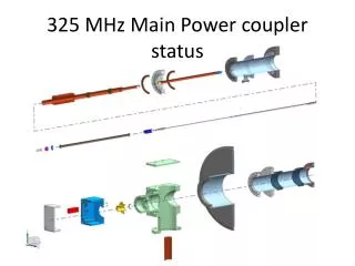
Design • Considering the short time available for the BEPCII construction, the high power input coupler is modified based on the KEKB 508MHz coupler. • In the following, some simulation works will be listed. 1. doorknob cover; 2. doorknob; 3. DC-bias component; 4. ceramic; 5. outer conductor; 6. inner conductor; 7. water-cooling pipes; 8, window; 9. monitor ports for vacuum、Arc and electron ; 10. BEPCII 500MHz superconducting cavity.
Window position The ceramic window is usually located at the minimum E-filed of the standing wave mode. Ceramic window
Tristan-type window optimization Conclusion: • The E-field near the choke tip increases obviously, so the distance from the choke tip to the ceramic surface should be carefully selected. • The H-field gratitude along the ceramic radius is high, especially the H-field on the inner conductor is quite high, so the dimension of the ceramic window inner conductor is not allowed to be too small.
Impedance matching optimization Conclusion: • ‘rw’, ‘h’, ‘r_doorkonb’ have a great impact to the central frequency; • the parameter “h” is changed to 94.5mm to shift the central frequency to 500MHz.
Qe calculation Conclusion: The results provide theoretical instruction for coupler input port design and the positioning of the antenna penetration depth.
Electron trajectory of the window : Multipacting simulation Tri-plots about the counter function, final impact energy of the window: Conclusion: By simulation, a one order MP appears on the vacuum side of the window at mixed wave mode.
Thermal simulation Calculated Dynamic losses Temperature distribution Thermal Stress distribution
Fabrication The fabrication flows of the inner conductor and the window:
Copper plating and TiN coating Copper plating A good sample (left) and a bad sample (right) of copper plating: bubbles on the bad sample due to too high current A plate shape Ti target acted as anode and the outer conductor of the window as the cathode. The desired film thickness is 8 nm. TiN coating
Steel- copper brazing AuCu(65%) at 1020 99.5% Al2O3ceramic- copper brazing Ag at 962 The whole window brazing AuCu(20%) at 889 , AgCu(28%) at 779 Copper- copper brazing AuCu(65%) at 1020 Brazingand welding
Brazing and welding, cont. TIG (Tungsten-arc inert-gas welding) EBW (electron beam welding) The ceramic shield before EBW (left) and after EBW (right)
Leakage checking and surface cleaning Final assembly leak check Subassemblies leak check OFHC parts after cleaning Assembly is processed in a class 100 clean room
Test Results The two key components (window and inner conductor) were fabricated in China and then received high power test in KEK. Professor Takaaki Furuya has given us great help about the test. The maximum power reached is 270kW in CW.
Test result (Cont.) No electron and outgasing were found at CW of 200kW after conditioning Keeping power test at 100kW ,150kW and 200kW Electron current state:
Part II: The preliminary consideration about the input coupler for IHEP 1.3GHz superconducting RF project
Through carefully investigating and considering our fabrication experiences, we choose the STF baseline type coupler as IHEP 1.3GHz coupler design prototype in the first research phase. IHEP 1.3GHz SCC coupler TTF III @DESY ERL @Cornell STF baseline型@KEK 电容型 @KEK
What have done • Preliminary RF structures have been calculated. • Coupling factor calculation has been finished decide the coupler port position Transition taper Cold part Warm part doorknob
Doorknob RF Structures Two parameters belong to the doorknob( highlighted with yellow) have been modified to get the optimum power transmission performance.
Warm Part RF Structures Warm window Try to reduce the number of bellows from 4 to 2: only one bellow on each conductors? Bellow
Cold Part RF Structures Cold window In order to match with the 40mm coupler input port, a tapper was used to transit the coaxial diameter from 60mm to 40mm.
E-field and H-field distribution 1MW @TW 1MW @TW Try to reduce the E-field on ceramic surface, especially air side.
RF Performance Maximum Mag_E on ceramic air side is 1.28e6 V/m, @ 1MW, TW, 115deg Power transmission performance Mag(S21)=0.9979@1.3GHz
Qe calculation • This work discusses the positioning of the high power input coupler for IHEP 1.3GHz 9-cell SCC. It examines the method used to reduce the model to enable faster solutions whilst still maintaining accurate results.
In order to faster solving, the model was reduced to 4.5-cell since Qe scales with the number of cells. The field flatness in every cell should be assured before the coupling analysis. Two parameters related with Qe were studied: 1) the coupler input port position; 2) the antenna penetration depth E-field distribution on Z-Plane Model of 4.5-cell and simplified coupler field magnitude along the on axis curve Parameters related with Qe
Qe calculation Plotted results • beam tube = 80mm • input port = 40 mm Distance from end-cell = ‘D’ The radius of antenna = 3mm Coaxial line = 50 W • To obtain the optimum 2×10⁶,we can: • Chose the distance from end cell to coupler port center D=40mm, adjust the antenna penetration near 4mm; • Chose the distance from end cell to coupler port center D=45mm, adjust the antenna penetration near 7mm; • Chose the distance from end cell to coupler port center D=50mm, adjust the antenna penetration near 10mm;
Part III: Some questions to be consulted
If the crest is wide enough (~2-3 mm), it may be able to support a MP buildup, or MP may jump across one MP resonance conditioned satisfied at operating power on flat wall Based on scaling, for a given bellows undulation or step, more MP resonances may be supported simultaneously, potentially increasing the conditioning area and gas load Question 1: Have you done MP simulation? 2D or 3D simulation? Tools?Did you find MP occurs inside the coupler, especially on the bellow area during high power test? How to avoid MP? Bellows or Steps May Lead to More Pervasive Multipacting “Coupler component Test stand Activities at SLAC/ LLNL”, TTC meeting @ KEK, WG1-input coupler, 2006
Question2: What’s the fabrication difficulties? • Copper Plating on Bellows? • Vacuum sealing of bellows? • Other?
Question3: About ceramic: • KEK coupler choose 95% Al2O3, why don’t you choose high purity ceramic? • Is the thermal shock tests of the ceramic necessary? Put into liquid nitrogen repeatedly: repeated times? Thermal Shock Test
Question4: Does the dimension shrinking from room temperature to cryo-temperature impact the power transmission performance? Why is the central frequency a little below 1.3GHz? Does it have relationship with dimension shrinking? My guess: Right? The RF structures simulated are at room temperature and after cooling down, the central frequency will shift to 1.3GHz.
Question5: Why does KEK STF coupler make a independent Vacuum in the inner conductor, since it results in DC bias impossible? Warm window Cold window Beam pipe 5K cooling Doorknob conversion 80K cooling Vacuum port Independent Vacuum? Why?
Questions 6 and 7:What kind of sealing gasket of flanges used between warm and cold parts, doorknob and warm parts connecting?What kind of method used in bellow connecting? Brazing or welding? What’s the method used in bellow connecting? What’s the sealing gasket of the flange?
Question8: Except copper plating, does the coaxial lines received other plating, e.g. ion plating? Plating method? Thickness? One of trial to reduce electron multipactoring amplitude, Ti ion plate with ~2-µm applied (gold color) to the inner and outer conductors for the coaxial transmission line. TTC at KEK
Question 9: When does TiN been coated on ceramic vacuum side? Before whole window assembled or after? What’s method used in TiN coating? TiN coating A A or B? B TiN coating
Question10:During brazing and welding, is there any metal vapor coming from? If there is, how to protect the ceramic? protection mask for ceramic and RF surface, TTF-III coupler e-beam for support and removal shielding against metal vapor ceramic with copper collars ERL mini-workshop at Beijing University, 7th – 8th November 2005
Question 11: Is it necessary to use four bellows? Why not just use two bellows (it’s similar with TTF-III coupler)? 4 bellows 2 bellows
Question 12: • what’s the stainless steel type? 316L or 316LN?