Download
1 / 41
410 likes | 577 Vues
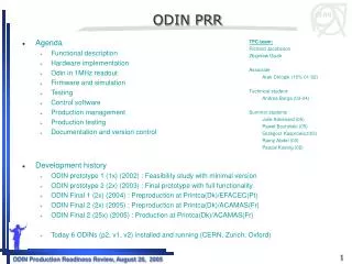
ODIN PRR. TFC team: Richard Jacobsson Zbigniew Guzik Associate Arek Chlopik (10% 01-02) Technical student: Andrea Borga (03-04) Summer students Julie Advenard (05) Pawel Bochinski (05) Grzegorz Kasprowicz(03) Ramy Abdel (03) Pascal Koenig (02). Agenda

E N D
ODIN PRR TFC team: Richard Jacobsson Zbigniew Guzik Associate Arek Chlopik (10% 01-02) Technical student: Andrea Borga (03-04) Summer students Julie Advenard (05) Pawel Bochinski (05) Grzegorz Kasprowicz(03) Ramy Abdel (03) Pascal Koenig (02) • Agenda • Functional description • Hardware implementation • Odin in 1MHz readout • Firmware and simulation • Testing • Control software • Production management • Production testing • Documentation and version control • Development history • ODIN prototype 1 (1x) (2002) : Feasibility study with minimal version • ODIN prototype 2 (2x) (2003) : Final prototype with full functionality • ODIN Final 1 (2x) (2004) : Preproduction at Printca(Dk)/EFACEC(Pt) • ODIN Final 2 (2x) (2005) : Preproduction at Printca(Dk)/ACAMAS(Fr) • ODIN Final 2 (25x) (2005) : Production at Printca(Dk)/ACAMAS(Fr) • Today 6 ODINs (p2, v1, v2) installed and running (CERN, Zurich, Oxford)
TTCmi Clock receiver/fanout LHC clock L0 (LVDS) L1 (GbE) Trigger splitter Local trigger L1(GbE) L1 L0 BPIM ODIN Readout Supervisor ODIN Readout Supervisor ODIN Readout Supervisor L0 MUNIN L0 Throttle Switch THOR TFC Switch L1 MUNIN L1 Throttle Switch TTCtx Optical transmitter TTCtx Optical transmitter TTCtx Optical transmitter TTCtx Optical transmitter TTCtx Optical transmitter TTC system TTCoc Optical splitter TTCoc Optical splitter TTCoc Optical splitter TTCoc Optical splitter TTCrx VELO L0 FE TTCrx ECAL L0 FE TTCrx TTCrx FREJA TTC monitoring TTCrx TTCrx TTCrx TTCrx VELO L0 FE VELO L0 FE VELO L0 FE VELO L0 FE VELO L0 FE VELO L0 FE TTCrx VELO TELL1 TTCrx ECAL TELL1 HUGIN L0 / L1 Throttle OR TTCrx TTCrx HUGIN L0 / L1 Throttle OR VELO L1 FE VELO L1 FE TFC Function
ODIN Bookkeeping DB Condition DB Configuration DB HLT farm Context diagram Beam Phase and Intensity Monitor Subdetectors LHC accelerator L1 trigger Beam Synch, Timing info (BST) Bunch currents MultiDecision Packets (MDP) Detector status HW and run parameters Run statistics Run conditions ‘Odin’ event bank
Block diagram L0 L1 Throttles LHC clock ECS Trigger generator ECS interface L1 broadcast generator Trigger rate controller Cmd broadcast generator Front-End TTC Encoder TTC Event building
Overall dataflow DETECTOR_STATUS L0_TRG L0_DATA FE_BUFFER Q_L0 FIFO BUNCH_INFO L0_TRIGGER FPGA Q_FE GbE GbE (EGRESS) L1_DATA L0_DATA L0_DATA AFIFO Q_L1 MEZZANINE FPGA GbE FIFO GbE (INGRESS) L1_TRG GPS L1_TRG Q_MP FPGA TTCrs TTC TTCrx LHC_TTC TTC_DATA L1BROADCAST & COMMANDS FPGA CIRCUIT MEZZANINE CLOCK ORBIT
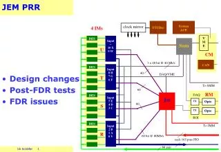
Front view Top layer Bottom layer 3mm 1.6mm 2.4÷2.7mm Hardware implementation • Design tools • Schematics and routing: Protel 99SE • Board dimensions • 9U VME • Same backplane as TELL1/UKL1 • ~2.7mm PCB • 1.6mm VME rails milling edges • Holes for rigidity bar (only one backplane connector) • Main FPGAs
Board Power • Use only +5V -5V, 3.3V, 2.5V and 1.8V made on board with regulators and DC/DC • Distribution of local power with split power planes • > 2 x calculated worst case consumption per regulator • Total 6.4A@5V (“idle”) / <9A@5V (“full operation”) • Board can survive for extended periods without cooling • Add cooling towers in TTC encoder, no need on regulators • Back plane / PC power connector • Power monitoring circuit • Range 4.7 V – 5.3 V • LED and status bit in FPGA
Board Control • Control Interface: CCPC and Glue light • Ethernet • I2C • JTAG • JTAG hub control • Local Bus • I2C • ~100 kHz • Five devices: • JTAG • ~100 kbits/s from CCPC • FPGA programming and boundary scanning in-situ • Fully configurable JTAG hub (programmed via header):
Board control • JTAG bus architecture • All TCK lines filtered by 74HC244 and serial 100 ohm resistors • TMS, TDI, TDO all have 33 ohm serial resistors
Board Control • Local bus • Configuring, controlling and monitoring all TFC functionality in the FPGAs • PLX 9030 Local Bus specification: • 32-bit synchronous multiplexed address/data • Bus clock: system clock (BCLK) / 2 : ~20 MHz • Bus clock and control lines re-driven with 74ALVC16244 line driver • Resets and other hardware control lines: • System reset set after power up • Reset of CCPC and Glue card • VME reset from backplane ( Row 17,18,19 (A=B=C) nSysReset) • Front panel push button
Board Control • Control of GbE MAC • Asynchronous u-processor bus • Conversion between Local Bus and MAC control bus inside FPGA • LBUS Address register for MAC internal register address • LBUS Data register for MAC configuration data • MAC reset vi control register in FPGA • Board id and code version • Board identifier stored in I2C EEPROM (0xA0) • Write protected (writing requires jumper) • FPGA code version • Local bus: (Main FPGAs: base address + 0xFC / Glue light : 0x3C) • YEAR(4) : MONTH(2) : DAY(2) : “HOUR”(2), that is for instance 2005071100
Board Control • TFC Control and Status registers • Local Bus registers in the main FPGAs • Configuration parameters • H_name : Hardware parameters linked to the actual installation (Set once-only) • P_name: Parameters configuring running modes and operation (may not be changed during data taking) • R_name: Run related parameters which either enable/disable functions or operate the data taking • Status registers • S_name : Status bit for a particular function • Distinction _INSTantaneous and _CONTinuous • C_name : Counter register • Reset registers • RST_name : Reset bits resetting individual functions • RST_CNT : Global reset of all counters and instantaneous status bits • RST_SEL_CNT : Selective reset of individual counters • Action registers • DMND_name : “Single-shot” bits to activate a function once on demand via ECS • UPDATE_CNT: Updates simultaneously all counter buffers for reading via ECS
Clock and orbit • Bunch clock • Two sources: External ECL AC coupled and internal ECL VXCO 80.158 MHz • PLL clock driver for 40MHz, 80MHz, 160 MHz (MPC991 obsolete) • Source selected by I2C • Fine phase adjustment: • LVPECL temperature compensated programmable delay chip 2.2ns – 12.2ns in 10 ps steps….(100EP195) • Controlled via I2C • Compensate for phase shifts monitored by Beam Phase and Intensity Monitor • Initial alignment with TTCrx’s(250 x 104ps) and equal cable lengths • Clock distribution as differential LVPECL using clock fan-out 100LVEP111 • Star to 10 destinations • Orbit signal • Two sources: External ECL DC coupled and internal generated in FPGA from BCLK • Source selected by the same I2C control line as for the bunch clock • External is routed to FPGA (differential LVPECL) for edge detection and re-generation • Re-generated bunch clock distributed to all FPGAs • Orbit signal may be shifted internally • In internal mode, orbit length is configurable…
TTC signal • TTC Encoder on board • Similar to TTCvx • Output is multiplexed A/B channel ECL AC-coupled • TTC signal is fanned out by THOR (TFC Switch) • Electrical to optical conversion by TTCtx
L0 Trigger Processing • L0 Trigger Flow • L0 throttle sources • External L0 throttle • ECS throttle • L0 derandomizer emulator • L1 Buffer Emulator • Gap generator • L0 Electronics Reset • L1 Electronics Reset • L0 Accept FIFO safety throttle • Front-End Buffer safety throttle • Automatic L0 trigger stop
L0 Trigger Processing • L0 Trigger Input • Parallel 16-bit LVDS with twisted pair flat ribbon cable and 3M HE-10 connectors (distance ~1m) • Implemented with MAX9179EUE • Clock/data alignment: • Latching on rising/falling edge • TTCrx in L0DU • L0 cable and TTC fibre length • Auxiliary L0 trigger input • Single-ended ECL DC-coupled via LEMO • L0/L1 throttle inputs • Dual twisted pair LVDS with RJ9 connectors • L0 Accept FIFO • Two 128K x 9bits discrete synchronous FIFOs CY7C4292V
L0 Trigger Processing • Front-End Buffer • Write 128 bits of L0 event data on every L0 trigger accept • 16 128K x 9bits discrete synchronous FIFOs CY7C4292V • Detector status input • Parallel 24-bit (2 bit/detector) LVDS with twisted pair flat ribbon cable and 3M HE-10 connectors • Signal directly sampled in FIFO, must be correctly aligned • Bunch Information Input (Bunch intensity) • General purpose 8-bit LVDS with twisted pair flat ribbon cable and 3M HE-10 connectors • Signal directly sampled in FIFO, must be correctly aligned
L0 Trigger Processing • GPS time • Received from Beam Synchronous Timing system via onboard TTCrx as long broadcasts • Extract 40 bits from 8 long broadcasts/turn with 8 bits (64 bits UTC) - ~ms resolution • 4 bits year • 9 bits day of the year • 17 bits second of the day • 10 bits milliseconds • GPS time is processed in Q_MP • Time shift added
L1 Trigger Processing • L1 Trigger Flow • L1 throttle sources • External L1 throttle • ECS throttle • L1 Electronics Reset • Trigger derandomizer safety throttle
L1 Trigger Processing • L1 Trigger Input • Gigabit Ethernet mezzanine SPI-3 bus operated at 80 MHz, PLL in FPGA • Voltage conversion for special control lines • Optional L1 Trigger input • Parallel 16-bit LVDS with twisted pair flat ribbon cable and 3M HE-10 connectors
Control Commands • TFC synchronous control commands generated by state machines • Bunch Counter Reset • L0 Event Counter Reset (L0 Event ID) • L1 Event Counter Reset (L1 Event ID) • Calibration pulse(s) • L0 Electronics Reset • L1 Electronics Reset • Periodic User command • TFC asynchronous control commands • L1 Triggers (accept interval 20 ms, reject interval 400ns) • L1 IP Destination (every n L0 trigger accepts) • HLT IP Destination (every m L1 trigger accepts)
Control commands • TTC transmission based on priority scheme • Request/acknowledge mechanism • Exact transmission time assured by forced pregap • Synchronous commands get postponed until next turn • Asynchronous commands get postponed until b-channel is free
L1 Front-End Processing • L1 Front-End data flow
Front-End Processing • Front-End Buffer read • FEB read in 8 clock cycles via 16 bit bus (pair of FIFO at a time) • ODIN Event Fragment 64 bytes • Data transmission • Gigabit Ethernet mezzanine Egress SPI-3 bus operated at 80 MHz (PLL in Q_FE).
ODIN in 1MHz readout • IP destination assignment, two schemes: • Static load balancing • Dynamic load balancing • Additional long broadcast for MEP synchronization • ODIN Event Fragment transmission at 1 MHz • Event fragment 68 byte • Bandwidth sufficient even with packing factor of 1 at 1MHz
ODIN in 1MHz readout scheme • Static load balancing
ODIN in 1MHz readout • Dynamic load balancing
Front-Panel • LEDs
Front-panel • Connections
Firmware and simulation • Tools • No particular tool for VHDL coding • Synthesis: Synplify • Placement and routing: Quartus • Simulation: Visual Elite • VHDL organization • Counters, RAMs and FIFOs using Altera LPMs Q_MP_v2: LBUS ODIN_orbit ODIN_bcr_ecr ODIN_ecr_internal ODIN_cal_trg ODIN_l0e_reset ODIN_l01e_reset ODIN_per_cmd ODIN_IP_broadcast ODIN_broadcaster ODIN_MP_counters ODIN_TTCrx Q_JTAGHUB_v2 Q_JTAGHUB_v2.vhd Q_FE_v2: LBUS ODIN_egress_pll Read_feb ODIN_read_feb ODIN_read_L1data ODIN_data_format ODIN_IP_handling ODIN_GBE_ctrl ODIN_DAQ_link ODIN_FE_counters Q_L1_v2: LBUS ODIN_L1_trigger_GBE ODIN_L1_trigger_LVDS ODIN_L1_internal ODIN_AFIFO_read ODIN_L1_synch_chk ODIN_L1_request ODIN_l1b_emulator ODIN_L1_counters Q_L0_v2: LBUS ODIN_bid ODIN_eid ODIN_L0_pipeline ODIN_L0_resynchronise ODIN_L0_synch_chk ODIN_handling.vhd ODIN_l0d_emulator ODIN_gap_generator ODIN_per_trg ODIN_rnd ODIN_L0_counters ODIN_bx_pipeline ODIN_bx_type
Based on Visual Elite 3.1.7 Includes LHC bunch generator, L0DU, L1DU, TTCrx, THOR, ODIN, FREJA, Front-End, Glue Heavily used and maintained up to date Functional and timing simulation Simulation AFIFO CCPC Q_L0 FEB Q_L1 Q_MP Q_FE GbE
Testing • Boundary scan • Local bus test • FIFO test • Gigabit Ethernet loop-back test • GbE(Ingress->Q_L1->Q_FE->GbE(Egress) • Loop-back tests with onboard TTCrx • FREJA emulating L0FE, L1FE, L0DU,L1DU • Full system operation with complete control system 4 ODINs installed in sub-detector tests (CERN, Oxford, Zurich)
Control software • Control operations via DIM • ReadWriteRegister(struct[]{method, address, data, mask, r/w}), • UpdateRegister(struct[]{address, data}), • SubscribeCounters(struct[] {address, interval}), • UpdateCounters(struct[] {address, data}), • FPGADownload(id, STAPL data), • FPGADownloaded(id, status). • On CCPC • I2C read/write • Local bus read/write • FPGA/EPC programming • GPIO control • Boundary scan • TFC server for PVSS control • Full TFC control system running centrally at CERN
Production management • Production archive • Company • PCB: GPV Printca (Denmark) • Mounting: ACAMAS (France) • Produce in total 25 boards • 2 x 2 pre-production • 6 production series PCBs made, in mounting • 19 boards to be produced
Documentation and versions • All to go in EDMS • Production archive to go in EDMS • Specifications • Technical Reference • … • Spare components