Memory Devices
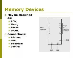
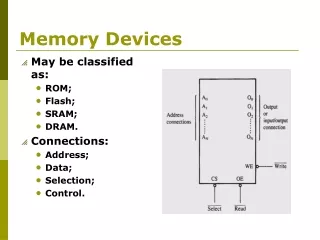
Memory Devices. May be classified as: ROM; Flash; SRAM; DRAM. Connections: Address; Data; Selection; Control. ROM – Read Only Memory. Combinational logic circuit. Non volatile type. Some do not think ROM is a memory device.

Memory Devices
E N D
Presentation Transcript
Memory Devices • May be classified as: • ROM; • Flash; • SRAM; • DRAM. • Connections: • Address; • Data; • Selection; • Control.
ROM – Read Only Memory • Combinational logic circuit. • Non volatile type. • Some do not think ROM is a memory device. • Others like to think the information is stored into the device in manufacturing.
ROM Application • A 4X4 multiplier may be designed by using a ROM whose inputs are defined as the multiplicand and the multiplier and the address they decode stores the product.
8X4 Diode ROM • Word line. • Each output of the decoder. • Bit line. • Each resistor terminated line. • What are the functions of the resistors and the diodes? • Address 5 (A2A1A0 = 101) has the value 2 stored in it.
8X4 Diode ROM • Notice that ROW3_L does not contain diodes, thus creating sneaky paths. • Now address 5’s output is modified by the new paths created by the absence of diodes in ROW3_L.
128X1 ROM • 3 to 8 decoder selects the word line. • 16X1 multiplexer selects the bit line. • Matrix of 23 X 24 locations.
ROM General Structure • Row decoder selects the word lines. • Column multiplexers selects the bit lines. • CS_L selects the device for operation. It is also used as a power down input. • OE_L enables the output buffer.
ROM Timing • tAA – Access time from address. • tACS – Access time from chip select. • tOE – Output enable time. • tOZ – Output disable time. • tOH – Output hold time.
Read/Write Memory • RWM – Read/write memory are memory arrays to which data may be written to or read from. • RAM – Random access memory are memory arrays whose time to read or write data is independent of the data location. • SRAM – data written to memory does not change unless overwritten or power is shut off. • DRAM – Data written to memory needs to be refreshed periodically. Data will be lost if it is not refreshed, it is overwritten or power is shut off.
Static RAM • Volatile. • Two access operations: • Read: • Address provided; • OE_L and CS_L asserted; • Data is read from memory cell at the address provided and made available at DOUT. • Write: • Address provided; • WE_L and CS_L asserted; • Data is written to the memory cell at the address provided.
8X4 Static RAM • Each cell is composed of a D latch and a NOR gate. • The array has a decoder to select the word line. • The output is buffered.
SRAM Read Timing • tAA – Access time from address. • tACS – Access time from chip select. • tOE – Output enable time. • tOZ – Output disable time. • tOH – Output hold time.
SRAM Write Timing • tAS – Address setup time before write. • tAH – Address hold time after write. • tCSW – Chip select setup before end of write. • tWP – Write pulse width. • tDS – Data setup time before end of write. • tDH – Data hold time after end of write.
Address Decoding • Addresses must be decoded to properly select a memory chip or port. • This decoded signal will select specific devices that will communicate with the processor through the data and control buses. • Several different methods may be used in address decoding: • Gates; • Decoders: • ROMs; • PLDs.

