Memory Devices
Memory Devices. Wen-Hung Liao, Ph.D. Introduction. Main memory vs. auxiliary memory. Memory Terminology. Memory cell : a device used to store a single bit (0 or 1). Examples: FF, charged capacitor, a single spot on a magnetic disk or tape.

Memory Devices
E N D
Presentation Transcript
Memory Devices Wen-Hung Liao, Ph.D.
Introduction • Main memory vs. auxiliary memory
Memory Terminology • Memory cell: a device used to store a single bit (0 or 1). Examples: FF, charged capacitor, a single spot on a magnetic disk or tape. • Memory word: a group of bits (cells) in a memory that represents instructions or data of some type. • Byte: a special term used for a group of 8 bits. • Capacity: a way of specifying how many bits of data can be stored in a particular memory device. Example: 4096 20-bit words = 4K x20 • Density: another term for capacity. Often with reference to space.
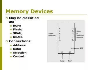
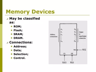
Memory Terminology(cont’d) • Address: A number that identifies the location of a word in memory. (Figure 11-2) • Read operation: the operation whereby the binary word stored in a specific memory location is sensed and then transferred to another device. • Write operation: the operation whereby a new word is placed into a particular memory location. • Access time: amount of time required to perform a read operation. • Volatile memory: any type of memory that requires the application of electrical power in order to store information.
Memory Terminology (cont’d) • Random Access Memory (RAM): memory in which the actual physical location of memory word has no effect on how long it takes to read from or write into that location. • Sequential Access Memory: a type of memory in which the access time is not constant but varies depending on the address location. • Read/Write Memory: any memory that can be read from and written into with equal ease. • Read-Only Memory(ROM)
Memory Terminology (cont’d) • Static memory devices: semiconductor memory devices in which the stored data will remain permanently stored as long as power is applied. • Dynamic memory devices: data need to be periodically refreshed. • Main memory: also referred to as the computer’s working memory. • Auxiliary memory: also referred to as mass storage. Always nonvolatile.
General Memory Operation • Select the address in memory that is being accessed for a read or write operation. • Select either a read or a write operation to be performed. • Supply the input data to be stored in memory during a write operation. • Hold the output data coming from memory during a read operation. • Enable (or disable) the memory so that it will (or will not) respond to the address inputs and read/write command.
Address Inputs • N words log2 N address inputs • The R/W’ input • Memory Enable: Chip Enable, Chip Select
CPU-Memory Connections • Address Bus: a unidirectional bus that carries the binary outputs from the CPU to the memory IC to select one memory location. • Data Bus: a bi-directional bus that carries data between the CPU and the memory IC. • Control bus: carries control signals from the CPU to the memory IC.
Read-Only Memory • Designed to hold data that either are permanent or will not change frequently. • During normal operation, no data can be written into a ROM, but data can be read from ROM. • The process of entering data is called programming or burning-in the ROM. • All ROMs are nonvolatile.
ROM Block Diagram • Figure 11-6 shows a 16x8 ROM. • 4 address inputs, 8 data outputs. • CS: Chip Select. • The Read operation.
ROM Architecture • Figure 11-7: architecture of a 16x8 ROM. • Register array • Row decoder • Column decoder • Output buffers.
ROM Timing • tACC: access time, time interval between the application of a ROM’s input and the appearance of the data outputs during a read operation. • tOE: output enable time, the delay between the CS input and the valid data output.
Types of ROMs • Mask-Programmed ROM: cannot be reprogrammed (Figure 11-9). • Programmable ROMs (PROMs): Figure 11-11. • Erasable Programmable ROM (EPROM): use UV lights to erase all cells at the same time. (15-20 minutes.) Vpp: programming voltage. Figure 11-12. • Electrically Erasable PROM (EEPROM): Figure 11-13, allows rapid in-circuit erasure and reprogramming of individual bytes, suffer from low density and higher cost. • CD-ROM
Flash Memory • Figure 11-14 shows the trade-offs for the various semiconductor nonvolatile memories.
Flash Memory (cont’d) • Flash memory aims to provide in-circuit electrical erasability, high-speed access, high density, low cost. • Erase mode: bulk erase, sector erase. • The 28F256A CMOS flash memory IC: Figure 11-15. • Figure 11-16: functional diagram of the 28F256A chip.
28F256A IC • Read command, Set-up Erase/Erase command, Erase-verify command, Set-up Program/Program command, Program-verify command
ROM Applications • Firmware • Bootstrap memory • Data tables • Data converter • Function generator • Auxiliary storage: flash memory.
Semiconductor RAM • When the term RAM is used with semiconductors memories, it is usually taken to mean read/write memory as opposed to ROM. • RAM is used for temporary storage of programs and data. • RAM is volatile. • Standby mode saves power.
RAM Architecture • Consisting of a number of registers, each storing a single data word, and each having a unique address. • Read operation • Write operation • Chip Select • Common input/output pins
Static RAM (SRAM) • Stores data as long as power is applied. • Static RAM timing • Read cycle (Figure 11-22a) • Write cycle (Figure 11-22b) • Actual SRAM chip: MCM6264 CMOS 8Kx8
Dynamic RAM (DRAM) • Needs to be refreshed every 2, 4,or 8 ms. • DRAM structures and operation (Figure 11-25,26) • Address multiplexing • DRAM read cycle (Figure 11-30) • DRAM write cycle (Figure 11-31)
Dynamic Memory Cell • WRITE operation: SW1,SW2 closed • READ operation: all closed except SW1
Address Multiplexing • 16Kx1 DRAM is obsolete. (has 14 address inputs) • 4Mx1 DRAM would require 22 address lines. • To reduce the number of pins on high-capacity DRAM, address multiplexing is utilized. • High-order bits row address • Low-order bits column address
RAS/CAS Timing • Row address strobe/column address strobe
DRAM Refreshing • DRAM chips are designed so that whenever a read operation is performed on a cell, all of the cells in that row will be refreshed. • Two refresh modes: • Burst refresh: normal memory operation is suspended, and each row of the DRAM is refreshed in succession until all rows have been refreshed. • Distributed refresh: row refreshing in interspersed with the normal operation.
Expanding Word Size and Capacity • Expanding word size: connecting two 16x4 RAMs for a 16x8 module. (Figure 11-34) • Expanding capacity: connecting two 16x4 chips for a 32x4 memory (Figure 11-36)
Special Memory Functions • Power-down storage • Cache memory • First-in, First-out memory (linear buffers) • Circular buffers