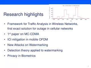
Research Highlights (1968-2006)
My Career at University of Florida Sheng S. Li, Professor Department of Electrical & Computer Engineering. Research Highlights (1968-2006). Background. Education: BS EE: National Cheng-Kung University, Taiwan, 1962 MS EE: Rice University, Houston, Texas, 1966

Research Highlights (1968-2006)
E N D
Presentation Transcript
My Career at University of FloridaSheng S. Li, ProfessorDepartment of Electrical & Computer Engineering Research Highlights (1968-2006)
Background • Education: • BS EE: National Cheng-Kung University, Taiwan, 1962 • MS EE: Rice University, Houston, Texas, 1966 • Ph.D.EE: Rice University, Houston, Texas, 1968 • Professional: (1968-2006 at UF) • Assistant Professor, 1968-73, E.E.Dept. • Associate Professor,1973-78 • Professor, 1978-2006 • Electronic Engineer, National Bureau of Standards (NBS), DC,1975-76 • Visiting Professor, National Chiao-Tung University, Hsinchu Taiwan,1995 (7 months)/2002 (1 month)
Books and Monographs • Semiconductor Physical Electronics (Plenum,1993) (S. Li) • Electrical Characterization of Silicon-on-Insulator Materials and Devices (Kluwer Academic,1995) (Li/Cristoloveanu) • Intersubband Transitions in Quantum Wells: Physics and Devices (Kluwer Academic, 1998) (LI/Su) • Semiconductor Physical Electronics (2nd edition, Springer, 2006) (S. Li)
Research and Scholarly Achievements (I) • Top 100Research Achievement Award, University of Florida, 1989 • Top 100Research Achievement Award, University of Florida, 1990 • Inaugural Professorial Excellent Program (PEP)award, University of Florida, 1996 • University of Florida Research Foundation's(UFRF)Research Professorship Award,2000-2003
Research and Scholarly Achievements (II) • Chair/co-chair of 2nd, 3rd, 5th, and 6th Int. Symposium on Long Wavelength Infrared Detectors and Arrays (1993,95’, 96’, 98’,99’ ECS Meetings) • Co-chair of Int. Workshop on Intersubband Transitions in Quantum Wells-Physics and Applications. (1997) • Editor/Co-editor of the above Conference Proceedings • Published 153 journal papers and 140 conference papers • Onemonograph book on SOI materials and devices • 3 book chapters on QWIPs (96’,99’,03’) • 2 NBS Special Publications (77’,79’) • Short courses: One in China two in Taiwan (90’,93’,02’) • Supervised 35 Ph.D. and 45 M.S. students
Highlights of Research • Studies of transport properties in semiconductor materials (DARPA,NBS, NSF, AFOSR) • DLTS characterization of radiation induced defects in GaAs solar cells and semiconductor materials (NASA) • Defect characterization in SOI materials and devices (Rome AFB, Harris Semiconductors) • QuantumWellInfraredPhotodetectors (QWIPs) for LWIR staring Focal Plane Array (FPA) applications. (1989-2004) (DARPA, ONR, AFRL, ARL, ARO, BMDO, ADT) • CuInSe2 (CIS) thin film solar cells. (1991-2006) (NREL)
Quantum Well Infrared Photodetectors (QWIPs) for Long Wavelength Infrared Imaging Arrays Fundamentals and Practical Applications
Applications of IR Detector Arrays • Automotive Industry • Weather Forecasting • Electronics • Infrared target detection • Astronomy Industrial Space Medical Military (MWIR)&(LWIR) (MWIR,LWIR)&VLWIR) (LWIR)
Applications of VLWIR (> 14 micron) Detectors • Deep Space • Astronomy • Atmospheric • pollution monitoring • Early detection of • long range missiles
QWIP Research Initiative • In 1990 DARPA issued a RFP called for the development of GaAs/AlGaAs QWIP FPA for LWIR imaging arrays applications • DARPA funded four research projects: UF (Li), AT&T Bell Lab, Rockwell, and Martin- Marietta) for 3 years to develop new QWIP devices and QWIP FPAs
(3-6 nm) MBE grown QWIP structure (GaAs)
Ec AlGaAs GaAs
• 1-D Time Independent Schrödinger Equation , z (growth direction of QW) and - Boundary Conditions : Continuities of • Transfer Matrix Method (TMM) - Calculations of energy levels and transmission coefficients A1 AN B1
• Absorption Coefficient: f (oscillator strength) • Light Coupling:Normal incidence absorption is forbidden in an n- QWIP. - 45o incidence for single detector and 1-D array detector - Grating coupler: 1-D (lamellar), 2-D (cross), random grating coupler. - C (corrugated)-QWIP - E (Enhancement) -QWIP
b GaAs Substrate
Calculated Peak Detection Wavelengths for an n-type GaAs/AlxGa1-xAs QWIP with AlAs Mole Fraction x GaAs/AlxGa1-xAs
Schematic diagram of the conduction band of a bound-to quasi-bound (BQB) transition QWIP under bias condition Absorption of IR photons can photo-excite electrons from the ground state of the quantum well into the continuum states, producing a photocurrent. Three dark current mechanisms are also shown: ground state tunneling (1); thermally assisted tunneling (2); and thermionic emission (3). The inset shows a cross-section transmission electron micrograph (TEM) of a QWIP sample. o
Photocurrent (1) Dark Current (A) (2) (3) Bias Voltage (V) • Dark currents (Id): (1) Thermionic emission (2) Thermally assisted tunneling (3) Direct or trap-assisted tunneling hn • Dark current calculation: (Thermionic emission):
• Spectral Responsivity (Ri) • Quantum Efficiency ( ) • Photoconductive Gain (g) •Detectivity (D* )
20 periods MWIR QWIPs 20 periods LWIR QWIPs Ec DE1 DE2 E1 DE2=0.124 eV, lp2=10 mm DE1=0.4 eV, lp1=3.1 mm lp (mm) = 1.24/DE(eV)
Conduction band diagram • of a TC-QWIP (b) Transmission coefficient of an InGaAs/AlGaAs/InGaAs TC-QWIP (a) Conduction band diagram and (b) transmission coefficient of a high- strain (HS) InGaAs/AlGaAs/InGaAs LWIR triple-coupled (TC-) QWIP. 18
5 periods 10 periods 19
Layer diagram of four-band QWIP device structure and the deep groove 2-D periodic grating structure. Each pixel represent a 640x128 pixel area of the four-band focal plane array
QWIP Technology for IR FPA 1. Advantages: • Highly uniform large format (640x480) GaAs/AlGaAs QWIP Focal Plane Array (FPA) can be fabricated for LWIR imaging array applications. • High yield and reproducibility using GaAs QWIP Tech. • Extremely low NEDT (10-20 mK/K) has been achieved in GaAs E-QWIP. 2. Drawback: • High dark current limits the operating temperature for QWIP to around 80K for 9mm detection peak.
0.5m GaAs, n=21018cm-3 Vb 600ÅGaAs (i) 10 In0.6Ga0.4As QDs 1m GaAs, n=21018cm-3 0.5m GaAs Buffer Semi-insulating (100) GaAs substrate An In0.6Ga0.4As/GaAs Quantum Dot Infrared Photodetector (QDIP) • A thicker spacer (600Å) of GaAs was • used instead of a larger band gap • material to block the dark currents. • Using a thicker spacer layer one could • reduce the dark currents without • blocking the photocurrent in the • QDIP.
Cross- Sectional TEM for an In0.6Ga0.4As/GaAs QDIP with High Operating Temperature (250 K) • Cross- sectional transmission electron microscopy (TEM) of the QDIP structure. • QD density is 1.21010 cm-2 • Average size of the QDs is 26 nm in diameter and 6nm in height • QDs grown by self-assemble mode using MBE techniques.
160K -0.7v 200K -0.6v 0.2v 180K RESPONSIVITY (mA/W) 200K 260K 220K 240K WAVELENGTH (m) Spectral Responsivity for an InGaAs/GaAs QDIP • Spectral responsivity vs. • wavelength measured • at 100 K to 260 K. • The bias voltages were • chosen to achieve the • maximum photocurrent • to dark current ratio.
QWIP Focal Plane Arrays (FPAs) using In- bump Bonding to Silicon CMOS MUX
QWIP Focal Plane Array Using In-bump bonding on Si CMOS MUX Twelve 640x512 QWIP focal plane arrays on a 3 inch GaAs wafer.
QWIP Phoenix Camera using JPL QWIP FPA Picture of the 640x512 hand-held long wavelength QWIP camera (QWIP Phoenix™). One frameof video image taken with the 9 µm cutoff 640x512 pixel QWIP Phoenix camera.
Recent Feedback from former students 1. Let me take this opportunity to thank you again for the positive impact that you have had on my life. I know that I was not the easiest student to deal with, but you were fair and flexible and helped me to complete my education in a positive way. I am sure that there are many students like me who you helped and who have made significant contributions to our industry. It is amazing to think of the change in the semiconductor industry over the last thirty years or so, and what total impact your students have made. Thanks again for letting me be a part of this industry- From Dr. Wade Krull (85’), Vice President, SemEquip, Inc. N Billerica, MA (email 4/10/06). 2. Congratulation to your retirement with great honor. You are such a great scholar and professor with warm heart. Even though I have been working with many engineers from the prestigious schools such as Cornell, MIT, Illinois, etc, the knowledge I learned from you is definitely world class and is my backbone and strength.- From Dr. K.C Hwang (90’), manager, Raytheon RF Component, Andover MA (3/9/06 email).