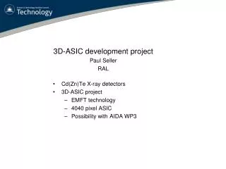
3D-ASIC development
3D-ASIC development. Rutherford Appleton Laboratory Mark Prydderch, Peter Murray, Matt Hart, Paul Seller. 3D-ASIC development. 3D-IC Upper pixel. The goal is to develop the next step in IC signal processing density for HEP, Synchrotrons, Space, medical…… systems

3D-ASIC development
E N D
Presentation Transcript
3D-ASIC development • Rutherford Appleton Laboratory • Mark Prydderch, Peter Murray, Matt Hart, Paul Seller Paul Seller :- AIDA EVO meeting 5/4/2011
3D-ASIC development 3D-IC Upper pixel • The goal is to develop the next step in IC signal processing density for HEP, Synchrotrons, Space, medical…… systems • Specifically a 3D-ASIC:- with two 2-D active layers bonded together at many points on surface • Layer 1:- Analogue preamplifiers • Layer 2:- Digital ADCs • Progress this year. • Define a Back-End-of-Line Process with EMFT so we could use different CMOS processes on the different layers. Cu/Sn SLID process with W vias. • RAL has designed and built the 2 layer CMOS wafers for EMFT (IZM Munich) bonding • 40 x 40 pixel ASIC for readout of pixel detectors 4040 pixel ASIC 3D-IC Lower pixel Paul Seller :- AIDA EVO meeting 5/4/2011
4040 RAL 3D-ASIC 3D-IC Upper pixel • Design • This circuit is copied from the Hexitec 8080 pixel CZT imaging readout • 250um pixels • 1-1.5keV FWHM with 2us shaping • Dynamic range to 150keV 8080 system with off chip ADCs Paul Seller :- AIDA EVO meeting 5/4/2011
4040 RAL 3D-ASIC • Lower layer has peak-hold and synchronous 12 bit ADC in every pixel. • Also identifies hit pixels and nearest neighbours • 1600 x 13 bits @ 50MHz = 0.4ms readout Schematic of lower layer pixel Paul Seller :- AIDA EVO meeting 5/4/2011
4040 RAL 3D-ASIC • Upper and lower ASIC on single wafer Paul Seller :- AIDA EVO meeting 5/4/2011
4040 RAL 3D-ASIC • Upper and lower pixels with via test areas clearly visible Paul Seller :- AIDA EVO meeting 5/4/2011
3D-ASIC development • Future plans 2011/2012. • 1) Test 2 layers separately with on-chip test circuits • 2) Start SLID bonding (2012 finish and test) • Require test effort and detailed design of SLID bonding • 125k Euro spent on design of 6 wafers • 25k Euro on 6 extra wafers • 165k Euro needed for EMFT • 315k Euro Total • 100k Euro request from AIDA:- for wafers, SLID and collaboration Paul Seller :- AIDA EVO meeting 5/4/2011
Detector eg. CZT Detector eg. CZT Wire bond Gold studs Gold studs 50um analogueASIC 50um analogueASIC SLID Bonds SLID Bonds Thick digital ASIC Thick digital ASIC Heat sink Heat sink PCB PCB Wire bond Very small dead space 3D-ASIC development • Advanced structure for 4-side butting. • Not yet discussed with EMFT Paul Seller :- AIDA EVO meeting 5/4/2011