Download
1 / 9
90 likes | 206 Vues
This document outlines the progress and challenges faced in the development of Application-Specific Integrated Circuits (ASICs) for the TGC electronics project discussed at the CERN meeting on June 21, 2002. Key updates include the submission and testing of various channel ASICs, resolutions of I/O pad misconnections, updates on master/slave logic for clock distributions, and assessment of performance from preliminary test results. The report emphasizes the adaptation of design features for compatibility and improved functionalities, targeting final production viability.

E N D
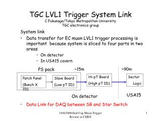
Status of ASIC development for TGC electronics JRC PPE SSW-rx VME protocol PP SLB Hi-pT Chikara FukunagaTGC electronics meeting on 21-June-2002 at CERN TGC electronics meeting at CERN June/2002
PP (Patch Panel) ASIC DLL →PLL • 16 chan. 0.35um VDEC 8/2001→3/2002 • 32 chan. 0.35um VLDAC (Rohm) 11/2001→4/2002 • 32 chan. version has been tested and found no analog circuits (lvds, PLL, Test pulse) worked. Upset & Struggle, and we found …. • Miss-connection of I/O pads. • The Analog I/Os have been connected to the digital I/O pads accidentally. • Each digital I/O pad has a digital CMOS buffer. Analog signals are blocked with the threshold of this buffer. • We have corrected already the pad miss-connection, re-submitted on 10-June, and expect to have new one in September (both 16- and 32- chan.) • We have used passport library for analog pads. TGC electronics meeting at CERN June/2002
SLB (Slave Board) ASIC • Version 1 (the first one after the premières ones used for the 2001 Slice test (= version 0)) has been submitted and tested preliminary. • 0.35um 10x10mm2 VLDAC (Rohm) 2/2002→Mid.6/2002 • New features • Standard JTAG, JTAG racing problem fixed (cDR < TCK problem) • New connection ordering with Hi-pT ASIC (Adapted to HpT ordering) • Clock distribution optimized (partially manual place and routing) • Clock bi-phase (master & slave) logic applied to PSC and JTAG • 32bit ID code • Test results (since only 1 week from delivery) • We have quickly checked the parts in which we had problems in 0-th version. • It would seem that almost all problems (in JTAG and readout) are solved with the above prescriptions. TGC electronics meeting at CERN June/2002
Hi-pT ASIC • Version 2 (to be final and fixed for the production ) • 0.35 um Hitachi Gate Array 12/2001→2/2002 • New features (Already reported in the last meeting in 2/2002) • 3-bit voting registers for delay control installed (JTAG accessible) • 32-bit ID code • Add New ID for No hit • Test results • A few thousands of I/O patterns (generated by the simulation) are checked for both wire and strip, and no problem found • Minor problem → Existence of Df value with >3 bits • Lowest 5 bits of output data consist of 1 bit for sign ± ,1 bit not used, and 3 bits for Df. • Non-used bit is not sent and simply suppressed to reduce the number of fibers. Df=-9 is expressed with the 5 bits as 01001, but data are sent as 0_001 (MSB 0 means negative, and _ means no connection) • Consequently at the receiver side, Df=-9 and Df=-1 are not distinguishable. • We plan to install an exterior circuit to deal Df > 3 bits as “No hit”. • We’d like to open PRR for Hi-pT in September 2002, either before or after LECC 2002 at Colmar. TGC electronics meeting at CERN June/2002
JRC (JTAG Route Controller) on PS-board • To ASIC from CPLD version used in Slice test 2001 • 2/2001→1/2002, and JTAG minor problem fixed, 2/2002→5/2002 • Now checking PPE (Primary Protocol Encoder for addressed JTAG access) on HSC • Transferred from CPLD to ASIC for radiation tolerance • Now checking SSW-rx (Star Switch Receiver) • Transferred from CPLD to ASIC for radiation tolerance • 2/2002→5/2002 • We will re-design the ASIC in the next fabrication VME protocol • Transferred from CPLD to ASIC for radiation tolerance • A24D16, VME slave access, no interrupt, no block mode transfer support • Used for both SSW and HpT VME modules • Under designing TGC electronics meeting at CERN June/2002