Download
1 / 17
170 likes | 201 Vues
Explore the advancements in epitaxial GaAs detectors for X-ray imaging, including growth, processing, and performance characteristics. Learn about overcoming limitations and historical developments in radiation detection with GaAs.

E N D
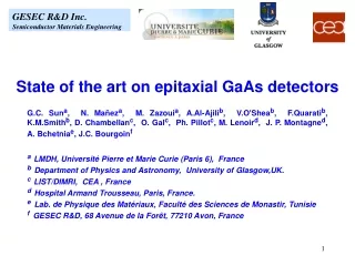
GESEC R&D Inc. Semiconductor Materials Engineering State of the art on epitaxial GaAs detectors G.C. Suna, N. Mañeza, M. Zazouia, A.Al-Ajilib, V.O'Sheab, F.Quaratib, K.M.Smithb, D. Chambellanc, O. Galc, Ph. Pillotc, M. Lenoird, J. P. Montagned, A. Bchetniae, J.C. Bourgoinf aLMDH, Université Pierre et Marie Curie (Paris 6), France bDepartment of Physics and Astronomy, University of Glasgow,UK. cLIST/DIMRI, CEA , France dHospital Armand Trousseau, Paris, France. e Lab. de Physique des Matériaux, Faculté des Sciences de Monastir, Tunisie f GESEC R&D, 68 Avenue de la Forêt, 77210 Avon, France
Motivation Decrease the dose (more than a factor of 10 compared to scintillator flat panels) in X-ray imaging
Outline • Review of X-ray detection with GaAs • Development of epi-growth of GaAs • Device processing • Device electrical characteristics • Performance of radiation detectors • Limitations of current devices and ways to overcome
History of GaAs radiation detectors (1) Early work with LPE GaAs (by Tavendale group, 1970) Three typical 241Am and 57Co -ray spectra, at 100V bias and 130K, from 1.5mm diameter, 80m thick LPE GaAs surface barrier detectors, (carrier concentration ~ 6 x 1013 cm-3), fabricated on tin-doped substrates.
History of GaAs radiation detectors (2) MBE epi-GaAs (Bertuccio et al., 1996/97) Pulse height spectrum of photons from an 241Am source detected in a 170 x 320m2 , 5 micron thick MBE undoped GaAs diode detector at 15V reverse bias
One 4 inch, 550 µm layer Thickness profile of epi-GaAs grown on four inch substrate Progress in the growth of epitaxial GaAs
SI GaAs Epitaxial GaAs layer CdTe Electronic properties of epitaxial GaAs • Photoluminescence mapping
ohmic contact p+ ion implantation (35 nm) GaAs epilayer n+ substrate (Cz GaAs) n+ ion implantation (35 nm) Technique to fabricate detectors
Current-Voltage characteristic of a small pad diode 2 nA/mm2 at 50 V
Combined source241Am(5.5 MeV), 244Cm (5.8 MeV) and 239Pu (5.2 MeV) Alpha particle pulse height spectra
Charge collection efficiency Fitted values at 100 V, giving charge collection efficiency of 85%.
Characteristic K-series X-rays of Ag, Ba and Nb. Pulse height spectra of monoenergetic X-rays
Photocurrent versus radiation dose 1mm2 epitaxial GaAs diode detector
Limitation: width of depleted zone Three ways to overcome it: • growth conditions • electron irradiation • use of 3D detectors
Before irradiation After irradiation 1 MeV electron irradiation Low defects not enough to compensate free carriers. Irradiation introduces defects increase depleted depth
3D detectors ‘3D’ SI-LEC GaAs pixel detector bonded to DASH-E ROIC