Download
1 / 62
630 likes | 749 Vues
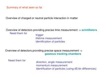
Summary of what seen so far. Overview of charged or neutral particle interaction in matter. Overview of detectors providing precise time measurement -> scintillators Need them for. trigger lifetime measurement identification of particles.

E N D
Summary of what seen so far Overview of charged or neutral particle interaction in matter Overview of detectors providing precise time measurement -> scintillators Need them for trigger lifetime measurement identification of particles Overview of detectors providing precise space measurement -> gaseous tracking chambers Need them for direction, angle measurement momentum measurement identification of particles (using dE/dx differences)
200 micrometers space point resolution is quite typical Gaseous tracking chambers Typical resolution ?
Radial : momentum measurement s=0.3 L2 B / 8 pT e.g. s=0.15 cm for pT =10 GeV (150 micrometers is resolution) so typically need L~ meters Longit. : have as much acceptance as possible to measure eg. differential cross sections, etc.. Depends on the goals of experiment. Typically ~ meters Gaseous tracking chambers What is the typical size (radial, longitudinal) at a collider experiment? Hint : what particle property do we want to measure ? and what polar angle distribution do we want to observe ?
Gaseous tracking chambers: literature W.Leo pages 119 - 146 D. Green pages 151 - 176 Peter’s notes on ISIS web site (all lecture slides are there !)
BaBar detector at Stanford Accelerator PEPII B0 electron positron Ecms=10 GeV Y(4S) -> BB =0.56 B0 Problem will be about evaluation of BaBar detector design
Babar physics goals which concern us today : - Measure very precisely the travel distance of the two B mesons - Measure very precisely the momentum of the particles coming from B meson decays Pros and cons ? Is the design appropriate to the physics goals? Can we suggest improvements?
The B meson travels a distance L and then decays into particles a and c > The impact parameter “b” particle “a” also carries information about the lifetime of the B meson. so it is important to be able to measure that too. What is the expected value for “b” ? (hint: assume small) a r c L b z B mesons (hadrons containing b quarks) have a mean lifetime = 1.5 picoseconds. At the PEP collider B mesons are produced with a boost factor ~ 0.5 > This means that they will travel on average a distance “L” = ? > What is the resolution needed to observe the decay length “L” and the impact parameter “b” ? We are happy if L / error(L) is > 3
A: L=average distance travelled in mean lifetime by B meson = c = 0.56 * 1.5 ps * 3 108 m/s= 230 micrometers b ≈ L if is small = pT /p of decay particle B ~ MB/2 / pB/2 ~ 1/()B => b ~ c = 450 micrometers a c L b to observe L at least a 3 sigma significance , meaning that L/error(L) >3, we need maximal resolution to be 70 micrometers. For b is 150 micrometers. Asking for 3 sigma is really the minimum, one should need more.
silicon So we need a different tracking device than the gaseous Ones, whose resolution is too coarse. Which one ? We need > Smaller resolution (electronic readout with higher granularity) > particles should loose little energy compared to initial energy > produce electronic signal high enough to detect particle and also fast enough to be readout before next collision event occurs Which one?
Goals of the lecture Silicon detectors Reference: D.Green, pages 177-201. W.Leo, pages Example of silicon detectors in past and current experiments Reference: slides (and web links) Exercise : Pros and cons of the BaBar detector? Vertex reconstruction and kinematic fitting. Reference : slides (and web links) Identification of heavy quarks Reference: slides (and web links)
Semiconductors devices (besides book reference, veryy usefull to browse here http://jas.eng.buffalo.edu/index.html)
Solid state or semiconductor detectors are made of crystalline semiconductor material, typically silicon or germanium
Development really started in 1950’s At first used for high resolution energy measurement and were adopted in nuclear physics for charged particle detection and gamma spectroscopy Last 20 years, gained attention in high energy physics for high resolution fast tracking detectors. Basic operating principle is similar to gaseous devices: charged particle ionizes and creates electron-hole pairs which are the collected by an electric field. Photons will also be detected in solid state detectors, via photoelectric effect and then electron ionizes.
Basic SemiConductor properties When isolated atoms are brought together to form a lattice, the discrete atomic states shift to form energy bands as shown below. Affects only the outer energy levels of atoms.
Intrinsic conductivity of semiconductors Thermal excitation of charge carriers across gap http://jas.eng.buffalo.edu/education/semicon/fermi/functionAndStates/functionAndStates.html
http://jas.eng.buffalo.edu/education/semicon/fermi/levelAndDOS/index.htmlhttp://jas.eng.buffalo.edu/education/semicon/fermi/levelAndDOS/index.html n = density of electrons in the conduction band = 1/V ∫ f(E) g(E) dE Where (density of states) n And similarly for holes (Reference : http://britneyspears.ac/physics/basics/basics.htm)
ni= concentration of e (holes). • Eg= energy gap at 0 Kelvin • Constantly : • e/h pairs are generated by thermal energy. • e and holes recombine. ni = AT 3/2 e (-Eg/2KT) equilibrium n electron= n holes in pure semiconductor ? e -Eg/2KT ~ 10-9 T=0, no conduction T=300 K, pure Si, 1.5 10 10 cm-3 (Remember there are 1022 atoms cm-3) -> Silicon is a poor conductor
Conductivity ~ 1/ resistivity If one applies a electric field E to a semiconductor, e and holes start moving. Drift velocity : ve = e E , vh = h E=mobility=f(E,T) T=300K , E<103 V/cm : is constant E ~ 103 - 104 V/cm : ~ E-1/2 E >104 V/cm : ~ 1/E saturation v=107 cm/s ~ T-m m=2.5 for e, 2.7 for holes in Si e = 1350 cm2/Vs in Silicon -> v= 1.3 106 cm/s (gas was 105 cm/s) J = current = e ni (e + h ) E
Recombination and trapping e can fall back into valence band, but need exact energy -> rare Nonetheless lifetime for e and holes is ~ ns -> what happens ? Impurities or defects in the semiconductor ! additional levels in the forbidden gap Recombination centre: This center can capture electron from conduction band and either release it back to the conduction band after a while or collect also a hole and e-hole annihilate Trapping center: This center can only trap an electron or a hole. They hold it and then release it after a while. http://jas.eng.buffalo.edu/education/semicon/recombination/indirect.html time electron is free should be >> time takes to collect electron out of detector -> impurity concentration should typically be < 10 10 impurities cm-3
Doped SemiConductors P-Type N-Type B, Al, Ga 3 electrons in the M-shell 1 electron missing P, As, Sb 5 electrons in the M-shell 1 electron with binding energy 10-50 meV .. When doping is actually good :)
0.05 eV in Si Fermi level much closer to conductive band or valence band Amount of dopant is quite small typically (10 13 cm-3). ND + n= NA + p In n type NA=0 , ND~n p= ni2 / ND -> conductivity is = e NDe Donor concentration determines conductivity
+ + Is this going to work? Can you foresee any Problems ? - - V … but how can we use a piece of Silicon for detecting a high energy particle … ?
We don’t like the thermal current ! Intrinsic silicon will have electron density = hole density ~ 1010 cm-3 In the volume above 4.5 108 free charge carriers But : only 3.2 104 produced by MIP (dE/dx in 300um Si divided by 3.6 eV). So, to use silicon as particle detector, we need to decrease number of free carriers How? - Reduce temperature ( need cryogenics, more expensive) - Create a free zone in the semiconductor
Reverse pn junction There must be a single Fermi level Deformation of band level Potential difference http://jas.eng.buffalo.edu/education/pn/pnformation3/index.html
Difference in concentration starts diffusion Perfect candidate for detector region
Solar cell Do we know an example of what a pn junction can be usefull for?
V is potential in figure f) of pn junction http://jas.eng.buffalo.edu/education/pn/pnformation3/index.html Field in a p-n junction is not intense enough to provide efficient charge collection thickness of the depletion zone will not be enough to detect high energy particles Solution: By applying an external voltage, we can enlarge the depletion zone and therefore the sensitive volume for radiation detection. The capacitance, hence the electronic noise, will also decrease
Reversed biased junctions http://jas.eng.buffalo.edu/education/pn/biasedPN2/BiasedPN2.html
The higher external voltage also helps increasing efficiency of charge collection. Max voltage appliable depends on the resistivity of the semiconductor. At some point junction will breakdown and begin conducting. In Si n-type, with V=300V a depletion d=1mm can be obtained Bigger d bigger resistivity (to postpone breakdown)
Signal from incoming particle Is readout p+ implant Si (n type) n+ implant Basic scheme for operating a pn junction p+n junction, depletion region all in the n region (as seen) To collect charge, electrodes must be placed on both ends. But the ohmic contact cannot be made by directly depositing metal on the semiconductor (else a rectifing junction extending into the semiconductor is formed). So heavily doped layers of n+ or p+ are used between the semiconductor and the metal. Typically, a preamplifier of charge-sensitive type, with low noise characteristics, is used to collect the charge out of the detector (~ 30000 eh pairs in 300 micrometers, need ampl.)
Leakage current Reverse biased pn junction does not conduct, ideally. In reality a small current always exists : leakage current. Appears as noise at the detector output. Sources: Movement of minority carriers (nanoAmpers/cm2) Thermally generated e/h due to impurities in depletion region (microAmp/cm2) Largest source: leakage current through surface channels. depends on a lot of factors (surface chemistry, contaminants, etc.) clean encapsulation is usually required http://jas.eng.buffalo.edu/education/pn/biasedPN/index.html
Intrinsic efficiency and sensitivity Basically 100%. Limiting factor on sensitivity is noise from leakage current (I) and noise from associated electronics ( C ) and thermal noise ( KT/R ) which sets a lower limit on the amplitude that can be detected Very important to choose correct depletion thickness, to ensure good signal
often require cooling to be operated, adds to material budget of detector To summarize
Silicon microstrip detectors pitch Voltage roughly 160 V
Q: Formula for resolution on position strip detector with pitch P=50 micrometers Q: what is the position resolution if the information saved is: which strip is hit ? Q: If one saves also the information: charge collected at each strip , can one think of improving the resolution ? P y
A: P y • 2 <(y - <y>)2 > = ∫ (y - <y>)2 dy / ∫ dy between -P/2 and P/2 (continuous form) assume uniform illumination given <y>=0 2 = ∫ y2dy /∫ dy = P2 /12 So if P=50m, then = 15m Reading out amplitude (of charge signal) at each strip, and weigthing positions with this, we can get better precision on position The position of the particle = the center of gravity of the charges collected at several readout strips.
Charge liberated by a charged particle is collected at the electrodes within 10 ns . Signals picked up at the strips measure the position with a precision dependent on the pitch of the strips. Detector with 20m pitch, readout every 6 or 3 strips. Resolution r is respectively : When Magnetic field applied !
Magnetic field (typically applied in high energy particle physics detectors) worsens the resolution and introduces a bias. Holes less mobile -> less angle One can improve by reading out more strips (every one, eg.). Simplified readout in this case if possible, to put on detector the electronics associated with each strip
fake real How to get 2-dim information
Solid state pixel detectors Avoids problem with combinatorics and gives precise 3-D information
Indeed we can clearly resolve decay distance “L” and impact parameter “b”
Disadvantage: Added material due to cryostat
Other examples of silicon detectors Reconstructed B decays DELPHI