NANO-TEXTURED MULTI JUNCTION SOLAR CELLS
40 likes | 236 Vues
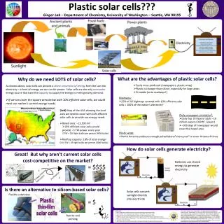
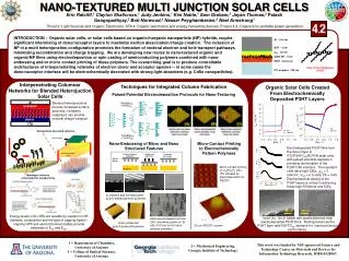
NANO-TEXTURED MULTI JUNCTION SOLAR CELLS. 1. Prepare Polymer and Mold. 2. Apply Heat and Force. 3. Separate and release. Silicon Master. Substrate. 20 μm. 20 μm. Al. acceptor. donor. ITO. Replicate. Master. top electrode. electron acceptor layer. 250 nm. 250 nm.

NANO-TEXTURED MULTI JUNCTION SOLAR CELLS
E N D
Presentation Transcript
NANO-TEXTURED MULTI JUNCTION SOLAR CELLS 1. Prepare Polymer and Mold 2. Apply Heat and Force 3. Separate and release Silicon Master Substrate 20 μm 20 μm Al acceptor donor ITO Replicate Master top electrode electron acceptor layer 250 nm 250 nm Erin Ratcliff,1 Clayton Shallcross,1Judy Jenkins,1Kim Noble,1 Sam Graham,2 Jayan Thomas,3Palash Gangopadhyay,3Bob Norwood,3Nasser Peyghambarian,3 Neal Armstrong1 Thrust 2: Light Sources and Organic Electronics, STA 4: Organic electronics and energy harvesting devices, Project 4.2: Organics for portable power generation INTRODUCTION : Organic solar cells, or solar cells based on organic/inorganic nanoparticle (NP) hybrids, require significant intermixing of donor/acceptor layers to maximize exciton dissociation/charge creation. The inclusion of NP in a multi heterojunction configuration promotes the formation of vectoral electron and hole transport pathways, minimizing recombination and charge trapping. We are developing new routes to nano-textured organic and organic/NP films using electrodeposition or spin casting of semiconducting polymers combined with nano-embossing and/or micro contact printing of these polymers. The overarching goal is to produce controllable architectures of interpenetrating networks of electron donor and acceptor species -- in some cases the donor/acceptor interface will be electrochemically decorated with strong light absorbers (e.g. CdSe nanoparticles). Al ~ 100 nm BCP ~ 5 nm C60 ~ 40 nm CdSe NP ~ 5 nm P3HT ~20-40 nm Poly (3-hexylthiophene) (P3HT) ITO on glass ~100 nm Interpenetrating Columnar Networks for Blended Heterojuction Solar Cells Techniques for Integrated Column Fabrication Organic Solar Cells Created From Electrochemically Deposited P3HT Layers Pulsed Potential Electrodeposition Protocols for Nano-Texturing Blended heterojunctions provide increased surface area and, if properly organized, can provide vectoral charge transport Nanoparticle decorated columns Nano-Embossing of Micro and Nano Structured Features Micro-Contact Printing to Electrochemically Pattern Polymers Electrodeposited P3HT films form the donor layer in ITO/P3HT/C60/BCP/Al solar cells, with pulsed-potential deposition providing texturization of the P3HT/C60 interface. The resultant cells have high IQEs, JSC = 3 mA/cm2; VOC = 0.5 volts, FF = 0.65. Electrochemical doping of the P3HT layers is critical in achieving these high fill-factors and IQEs. Micro contact printing of C18PO3H2 onto ITO followed by electrodeposition of PEDOT. Monolayer-tethered semiconductor nanoparticles Master Replicate Si masters and hot embossed poly(3-alkylthiophene) polymers Energy levels in SC-NPs are tunable by variation in NP diameter, composition and the type of capping ligand – ongoing UPS and electrochemical studies provide estimates of EVB and ECB. SEM (45° tilt) of carpet and pulsed potential step electrodeposited P3HT films. Pulsing texturizes the P3HT layer and P3HT/C60 interface for improved device performance. ZnO nanowires grown on Si (dia~100 nm) to hot nano-emboss polymers. Nano-patterned poly(3-dodecylthiophene) 20 mm PEDOT column 1 = Department of Chemistry, University of Arizona 3 = College of Optical Sciences, University of Arizona This work was funded by NSF sponsored Science and Technology Center on Materials and Devices for Information Technology Research, DMR-0120967. 2 = Mechanical Engineering, Georgia Institute of Technology