Download
1 / 1
10 likes | 221 Vues
(a). Electrochemical formation of Porous Silicon in Room Temperature Ionic Liquid. O. Raz , D. Starosvetsky and Y. Ein-Eli. Corrosion & Applied Electrochemistry Laboratory (CAEL) Department of Materials Engineering, Technion, Haifa 32000, Israel.

E N D
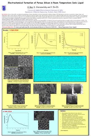
(a) Electrochemical formation of Porous Silicon in Room Temperature Ionic Liquid O. Raz, D. Starosvetsky and Y. Ein-Eli. Corrosion & Applied Electrochemistry Laboratory (CAEL) Department of Materials Engineering, Technion, Haifa 32000, Israel. Introduction: Porous Silicon (PS) can exhibit rich morphological features depending on various experimental conditions (doping of the bulk material, electrolyte concentration, etching volume, and temperature). Macro-porous silicon is defined as silicon having pores in the micro-metric range. This material was the first to have commercial applications in the capacitor technology and it is investigated as a material for micro-system technology and serves as an electrode based material. PS is usually formed by the application of low anodic bias on the silicon substrate immersed in a solution containing HF. PS is also formed in electrolytes containing HF and an organic solvent (water addition, originated from HF (49%), is always included in the electrolyte composition). Such as, acetonitrile (MeCN), dimethylformamide (DMF), dimethylsulfoxide (DMSO), ethanol and others, as well. A novel study on the electrochemical interaction between silicon and room temperature ionic liquids (RTIL’s) is reported. This novel research provides new insight on silicon electrochemistry in RTIL’s. The research is in designed RTIL’s, with desired properties: wide electrochemical window and high conductivity. As a part of this study is understanding the electrochemical behavior of silicon in a new and novel RTIL based on 1-ethyl 3-methyl imidazolium (EMI) cation with (HF)2.3F- anion. This RTILis non aqueous and exhibits high conductivity (100 mS cm-1), and is considered acidic and hydrophobic. Formation of a Porous Silicon by application of a positive potential on both n and p type Si in EMIF(HF)2.3 is presented. The effect of time and potential on Porous Silicon formation and structure will be discussed These results are important towards the understanding of the unique silicon dissolution mechanism, by performing it in a non-aqueous media. Research objectives: Tostudy and understand the electrochemical behavior of silicon in EMIF(HF)2.3Room Temperature Ionic Liquid.. n-type silicon Results: Figure 1: Anodic potentiodynamic curve of n-Si in EMIF(HF)2.3 , Scan rate 5 mV/sec, 25oC. Figure 3: 8V anodic polarization potentiotiostatic study of n-Si in EMIF(HF)2.3 Figure 2: 8V anodic polarization potentiotiostatic study of n-Si in EMIF(HF)2.3 Discussion: Figure 1 presents potentiodynamic studies of n-Si in EMIF(HF)2.3 in anodic polarization. currents of up to 100 mA/cm2 were developed. The high currents, generated in EMIF(HF)2.3 RTIL are mainly due to the high conductivity and low viscosity of this particular RTIL. Potentiostatic curve obtained from polarizing n-type silicon at a potential of 8V in EMIF(HF)2.3 obtained at different polarization periods are shown in Figure 2. The current increases to a maximum value of 150 mA/cm2 within 15 minutes followed by a gradual decrease, to 20 mA/cm2 after 3 hours. This current is maintained low during the rest of the experiment time. During the experiments, gaseous products are emitted and the solution color changes, from transparent to brown. Figure 4 presents the formation of pores at the silicon interface. Within 15 minutes, pits are being formed at the silicon surface, and as time progresses pores are being formed. At a longer time period, the silicon porous structure becomes less uniform. Figure 3 presents potentiostatic curves obtained from polarizing n-type silicon at different potentials in EMIF(HF)2.3 for ten hours period. In all the curves there is an increase in the current up to a maximum value followed by a gradual decrease. The maximum current is increased as the potential applied is increased. Figure 5-7 shows top, tilted and cross section views of n-type silicon after ten hours study at different potentials. 8V study shows less uniform structure with pores with ~1mm wide and ~10mm wide. 5V study tilt view shows less uniform bundle structure than the 2V study. The cross section view shows longer pores length at the 2V samples (20 mm) compared to the 5V sample (5mm), these pores are thinner as the pore is deeper. Figure 8 presents potentiostatic curve obtained from anodic polarization of n-type silicon in EMIF(HF)2.3 at a potential of 8 V. It shows an increase in the current value, until a maximum current value of ~60 mA/cm2 is reached after one hour. During the experiments gas is evolved and the solution color is changed from transparent to brown. The recorded current is low, compared with experiments conducted with n-type silicon. Figure 9 presents silicon surface morphology subsequent to different experiment time periods. After an hour texturing of the surface is observed. This texturing is probably developed at a later stage (longer time periods). A cross section of these samples will be studies, as well. The difference between the morphology developed with n and p-type silicon will be investigated in this research. A possible mechanism for the formation of the porous structure is provided here and should be verified during this study; the oxidation product or products of the anion are in-charge of the pore formation. This oxidation leads to a change in the hydrofluoric anion structure. Thus it is reasonable to assume that some of the anion molecules are dissociated to produce free HF, which is “available” to react with the silicon surface, leading to the formation of pores. Finding the mechanism for this reaction and the oxidation products which are formed and responsible for this process is one of the main goals of this research Figure 4: SE micrographs of n-type Si (100) subsequent to exposure to a potential of 8 V (anodic polarization) in EMIF(HF)2.3; (a) 15 min, (b) 30 min, (c) 3 hr, (d) 10 hr. Figure 6: SE micrographs in 52o tilt view of n-type Si (100) subsequent to exposure to anodic polarization in EMIF(HF)2.3 for 10 hr; (a) 2V, (b) 5V, (c) 10V. Figure 7: SE micrographs of crooss section view of n-type Si (100) subsequent to exposure to anodic polarization in EMIF(HF)2.3 for 10 hr; (a) 2V, (b) 5V, (c) 10V. Figure 4: SE micrographs in top view of n-type Si (100) subsequent to exposure to anodic polarization in EMIF(HF)2.3 for 10 hr; (a) 2V, (b) 5V, (c) 10V. p-type silicon Summery • Electrochemical dissolution of n-type silicon in EMIF(HF)2.3 leading to the formation of porous silicon under anodic polarization is presented. • Increasing experiments results in porous structure formation, which becomes less uniform with time. • Increasing the potential from 2V to 5V results in deeper pores formation, while 8V experiments show wider pores. • Also, cathodic polarization of p-type silicon in EMIF(HF)2.3 leads to electrochemical dissolution • Finding the mechanism responsible for electrochemical dissolution of silicon in EMIF(HF)2.3. • Further studies will be conducted in order to determine the mechanism responsible for these results. Acknowledgements: Figure 9 :HRSEM obtained from p-type Si (100) subsequent to exposure at a potential of 8V in EMIF(HF)2.3; (a) 1 hr, (b) 5 hr, (c) 8 hr. Figure 8 : Potentiotiostatic profile of p-Si (100) in EMIF(HF)2.3performed at 8 V.