Download
1 / 25
270 likes | 488 Vues
An Electrochemical Etching System for Producing Porous Regions in 100 mm Diameter Silicon Wafers. Containing a Finite Element Analysis ( FEA ) using flexPDE. Craig E. Nelson - Engineer. Introduction.

E N D
An Electrochemical Etching System for Producing Porous Regions in 100 mm Diameter Silicon Wafers Containing a Finite Element Analysis ( FEA ) using flexPDE Craig E. Nelson - Engineer
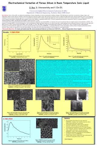
Introduction The etching cell system described in this report is used to create porous regions in 100 mm N type silicon wafers. In order for porous regions to be created, an electric current must be passed through the silicon wafer while it is immersed in an ionically conducting electrolyte solution. The current and electrolyte must be well controlled in order for the resultant porous regions to have well defined and desirable qualities. Because N type silicon does not, of itself, contain enough of the current carriers needed for satisfactory pore creation, they must be created artificially by means of an auxiliary process. The process used is based on the electro-physical phenomenon of photon absorption. This process results in current carrier creation at the point of absorption within the silicon crystal lattice such that anodic etching may proceed in a manner that produces desirable porous silicon regions within the wafer. In order for the porous silicon process to proceed, several subsystem elements must be set in place: 1 An etching cell housing to contain and channel the electrolyte while maintaining the electrodes and silicon wafer in useful relative position. 2. A source of optical illumination to create current carriers with the silicon wafer by photon absorption. 3. A fluid handling system to store, pump and temperature regulate the electrolyte. 4. Electronic power supplies to drive the optical illuminator and electro-chemical etching process. 5. A data acquisition system to monitor the etching process parameters. 6. A host computer to control the etching process and record relevant data. 7. Software to execute the system hosting, monitoring and data recording functions. Additionally, the etching cell system needs a physical place wherein to reside. The electronics and host computer are conveniently located in a standard electronics rack and the etching cells and fluid handling system are located within a set of two wet benches of the kind typically used for chemical work.
An Early System Developed at the University of Kiel Electrolytic Etching Cell Power Supply Infrared Light Source Power Supply System Host Computer Etching Cell
Small Electrolytic Etching Cell Developed at the University of Kiel
Electrolytic Etching Cell Fluid Dynamics a Finite Element Analysis ( FEA ) Using FlexPDE
Partial Differential Equation Formulation for Fluid Dynamic Finite Element Analysis (FEA) Although this equation is consistent with the continuity equation, it does not enforce it. However, since div[U,V] = 0, we are free to add it at wil to the pressure equation. A negative value of div[U,V] implies the destruction of material, so we need a positive pressure to oppose the flow. This implies a modified pressure equation del2(P) = 2*dens*[dx(U)*dy(V) - dy(U)*dx(V)] + L*(dx(U)+dy(V)) where L is a "large" number chosen to enforce "sufficient" compliance with the material conservation equation. Setting U and V equal to zero in the U and V equations to reflect the conditions on a no-slip boundary, we get dx(P) = visc*del2(U) dy(P) = visc*del2(V) These relations can be used to specify the natural boundary condition for the pressure equation. The normal component of the gradient of P is n<dot>grad(P) = nx*dx(P) + ny*dy(P) where nx and ny are the direction cosines of the surface normal. The Navier-Stokes equation for steady incompressible flow in two Cartesian dimensions is dens*(dt(U) + U*dx(U) + V*dy(U)) = visc*del2(U) - dx(P) + dens*Fx dens*(dt(V) + U*dx(V) + V*dy(V)) = visc*del2(V) - dy(P) + dens*Fy together with the continuity equation div[U,V] = 0 where U and V are the X- and Y- components of the flow velocity P is the fluid pressure dens is the fluid density visc is the fluid viscosity Fx and Fy are the X- and Y- components of the body force. In order to derive a third equation for the Pressure variable, we differentiate the U-equation with respect to X and the V-equation with respect to Y. Using the continuity equation to eliminate terms, we get del2(P) = 2*dens*[dx(U)*dy(V) - dy(U)*dx(V)]
Electrolyte Outlet Pots Electrolyte Inlet Ports Line of Symmetry Inlet Side Outlet Side Electrolytic Etching Cell Velocity Magnitude Distribution – FEA analysis using flexPDE
Electrolytic Etching Cell Velocity Distribution – FEA analysis using flexPDE
Electrolytic Etching Cell Velocity Distribution - Expanded – FEA analysis using flexPDE
Electrolytic Etching Cell Pressure Distribution – FEA analysis using flexPDE
Installed System – Host Computer, Power Supplies and Etching Cells in a “Hood”
Installed System – Host Computer and Etching Cell Power Supplies
Summary and Conclusions An electrolytic etching cell suitable for producing 100 mm diameter porous silicon wafers has been designed and presented. Creation of the system required top down design of unique infrared illumination, fluid distribution and electronic control subsystems. The overall design and the detailed design of the individual subsystems was successful and many hundreds … perhaps thousands of porous silicon wafers have been fabricated.