GEM basic test and R&D plan
GEM basic test and R&D plan. Takuya Yamamoto ( Saga Univ. ). Introduction. GEM is used for the sensor part of TPC. Beam test that examined a basic performance of GEM was done. GEM. Fuchigami GEM. 70μ m. 70μ m. 60μ m. 140μm. 10cm. CERN GEM. 5μ m( Cu ). 50μ m ( KAPTON ). 5μ m( Cu ).
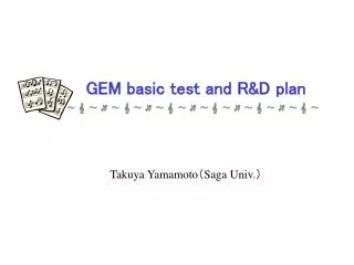

GEM basic test and R&D plan
E N D
Presentation Transcript
GEM basic test and R&D plan Takuya Yamamoto(Saga Univ.)
Introduction GEM is used for the sensor part of TPC. Beam test that examined a basic performance of GEM was done.
GEM Fuchigami GEM 70μm 70μm 60μm 140μm 10cm CERN GEM 5μm(Cu) 50μm (KAPTON) 5μm(Cu)
Outline of BEAM TEST Transfer area 2kV/cm 1.5mm Induction area 3kV/cm 1mm 6mm 2mm Compares of CERN and Fuchigami. • Used and tested at Hiroshima Univ. Refer • 150MeV Electron Beam • Three GEM was installed in the chamber. • The gas used the P-10 gas. • Reading PAD was used the one of PrototypeTPC. • The trigger counter was set up back and forth. Dielectric board (Cathode) Drift area 213V/cm 235mm GEM3 GEM2 GEM1 PAD GND (Anode) The space between PAD is all 0.3 mm.
Residual Fuchigami 1000 Events Residual = C.O.G.-Track [μm] σ ≒320 [μm] m -2 -2 0 0 2 2 Residual [mm] CERN 350 Each of Layer4 Positional resolution Events Fuchigami GEM 290μm σ ≒380 [μm] m CERN GEM 340μm Residual [mm] 400 180 Events Events 100 200 - 3 0 4 0 4 - 3 Track [mm] C.O.G. [mm] ( Fuchigami GEM : Layer4 (VGEM=330(V) )
Track / Residual -3 -3 0 0 4 4 CERN Fuchigami Residual [mm] Residual [mm] 2 2 0 0 - 2 - 2 Track [mm] Track [mm] Fuchigami GEM : Layer4 (VGEM=330V) CERN GEM : Layer4 (VGEM=330V) Systematic behavior is seen
Size of electron distribution • Response Function Distribution of charge seen from each pad of one layer. 100 100 Ratio of charge (%) Ratio of charge (%) 50 50 0 0 -4 0 4 -4 0 4 Fuchigami Distance from PAD to Track(mm) Distance from PAD to Track(mm) CERN Fuchigami GEM : Layer4 (VGEM=330V) CERN GEM : Layer4 (VGEM=330V)
Difference of pulse height sumADC ●CERN 〇 Fuchigami events Fuchigami CERN ADC counts 1count = About 0.25pC Pad raw No. (Layer) The gain of Fuchigami GEM is about 0.8 times CERN GEM. Fuchigami GEM :Layer4 (VGEM=320V) CERN GEM :Layer4 (VGEM=320V)
Result of BEAM TEST • Fuchigami GEM operated as well as CERN GEM , too • Obtained Position resolution (Non Magnetic field) • FuchigamiAbout 290[μm] • CERNAbout 340[μm] In SN influences • Some problems happened during Beam test
In developing • The durability of GEM Normal Discharged GEM(CERN) Damaged
Durability of GEM When HV is raised and beam ON, GEM is discharged. Hypothesis When the numbers of ions collected in the hole increase too much, and copper is transformed. As a result, it energizes between both electrodes.
Development of GEM① • To investigate the cause of the electrical discharge, the segment does GEM. 10cm Possible to impress HV to nine separate GEM
Development of GEM② • We try Nickel coated GEM. Nickel
Development of GEM③ • The load of one hole is decreased by increasing the number of holes. 9cm 3cm • The diameter of the hole is 30μm. • Laser etched by 50μm pitch. Some surfaces are uneven because of the heat of the laser.