Run IIb Silicon Meeting Summary: Progress, Milestones, and Future Goals
40 likes | 159 Vues
The Run IIb Silicon Meeting, held on November 19, 2002, addressed current progress on key projects including radiation and temperature monitoring systems. Key near-term milestones were highlighted, such as sensor probing equipment setup, and the decision on final stave design. Attendees discussed issues affecting the schedule and outlined goals for an upcoming workshop on technical design proposals. Coordination efforts for sensor tests and a coherent overall design were emphasized to ensure successful outcomes in ongoing and future work.

Run IIb Silicon Meeting Summary: Progress, Milestones, and Future Goals
E N D
Presentation Transcript
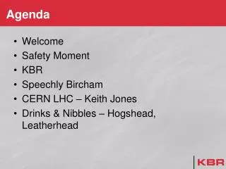
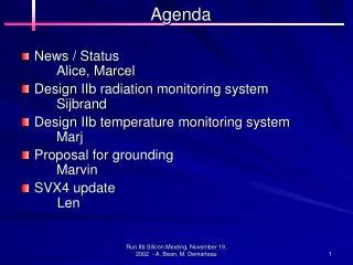
Agenda • News / Status Alice, Marcel • Design IIb radiation monitoring system Sijbrand • Design IIb temperature monitoring system Marj • Proposal for grounding Marvin • SVX4 update Len Run IIb Silicon Meeting, November 19, 2002 - A. Bean, M. Demarteau
Schedule • Near term milestones • 1.1.1.1.3 Sensor Probing Equip Setup And CertF. Complete 11/6/02 • Missed • 1.1.3.11.4 Silicon Prototype Mechanical Stave Built Mon 12/16/02 • Major milestone at which point final stave design will be chosen • 1.1.1.2.4 Choose Layer 0/1 sensor technology 2/5/03 • 1.1.1.4.2.2.2 Order outer layer sensors 2/11/03 • Tasks having started / ending this month • 1.1.1.2.1 Develop Layer 0 Masks 11/27/02 • 1.1.2.4.2.3 Testing Layer 2-5 hybrid prototypes 10/27/02 • 1.1.2.16.1.1 Design IB backplane prototype 3/7/03 • 1.1.2.17.1.1 Design Low Voltage System 2/21/03 • 1.1.3.2.7 Engineering prototype L0 support structure 3/10/03 • 1.1.3.3.6 Engineering prototype L1 support structure 3/14/03 • 1.1.3.4 Layer 0 Tooling Fabrication 12/3/02 • 1.1.5.2.1.1 Prototype shells for support cylinders 11/25/02 • 1.1.6.2.1 Design Radiation Monitoring System 11/25/02 • 1.1.7.4.1.1. Modification of 2a Unpacking Code 10/30/02 Run IIb Silicon Meeting, November 19, 2002 - A. Bean, M. Demarteau
News and Status • Schedule • We are lagging in several areas. At the next L3 meeting we would like to address these areas • At the L3 meeting we will also discuss schedule status and effort reporting Run IIb Silicon Meeting, November 19, 2002 - A. Bean, M. Demarteau
Workshop • Date: Dec. 12 and 13 • Workshop: “Moving beyond the Technical Design Proposal” • We are close to making some decisions regarding the final configuration of various detector elements. Moreover, some significant milestones are coming up; we should prepare ourselves for PRR’s and identify any possible shortcomings in our current testing and/or design, ensure a coherent design and provide documentation • Goals: • Full overview of layer 0 and Layer 1 sensor tests, irradiation tests; decide on layer 0 sensor/hybrid configuration • Full review of outer layer sensor probing results • Will try to do sensor discussion together with CDF • Evaluation of stave design • Presentation of design for Low Voltage system • Fully worked out plan for horseshoe area, including infrastructure needs • Plans for junction card area layout and run to horseshoe area Run IIb Silicon Meeting, November 19, 2002 - A. Bean, M. Demarteau