A Novel Time- Area-Power Efficient Single Precision Floating Point Multiplier
170 likes | 781 Vues
A Novel Time- Area-Power Efficient Single Precision Floating Point Multiplier. Himanshu Thapliyal and M.B Srinivas (thapliyalhimanshu@yahoo.com, srinivas@iiit.net) Center for VLSI and Embedded System Technologies International Institute of Information Technology

A Novel Time- Area-Power Efficient Single Precision Floating Point Multiplier
E N D
Presentation Transcript
A Novel Time- Area-Power Efficient Single Precision Floating Point Multiplier Himanshu Thapliyal and M.B Srinivas (thapliyalhimanshu@yahoo.com, srinivas@iiit.net) Center for VLSI and Embedded System Technologies International Institute of Information Technology Hyderabad-500019, India
Abstract • In this paper, a Single Precision IEEE 754 floating-point multiplier with high speed and low power is presented. • The bottleneck of any Single Precision floating-point design is the 24x24 bit integer multiplier. • Urdhava Triyakbhyam algorithm of ancient Indian Vedic Mathematics is utilized to improve its efficiency. • In the proposed architecture, the 24x24 bit multiplication operation is fragmented to four parallel 12x12 bit multiplication modules. • The 12x12 multiplication modules are implemented using small 4x4 bit multipliers. • In the unsigned 24x24 bit multiplier architecture, four redundant 4x4 multiplier are provided to enforce the feature of self repairability (to recover from the faults in each 12x12 multiply modules) . • Reconfigurability at run time is provided for attaining power saving . • The multiplier has been designed, optimized and implemented on an FPGA based system. • Thus, a highly regular, self-repairable floating point parallel multiplier architecture (which can be directly scaled for larger multiplication ) is proposed.
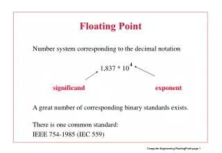
INTRODUCTIONIEEE 754 standard for floating point Sign bit 8 bit exponent 23 bit Mantissa Normalized form 1.b1b2b3……….b23*2exp Hidden bit
Addition • Subtract Exponents • Compare • Right Shift Significand with smaller exponent • By difference • Add/Subtract Significands (sign bits) • Normalize • Shift significand • Add or Subtract shift amount to exponent • Round • To number of bits for significand • Need to keep extra bits during computation
Addition 8-Bit Sub 24-Bit ALU Control MUX MUX MUX MUX MUX 1 1 Exp Diff Shifter Normalize Inc/Dec Shifter Round
8-Bit Add 8-Bit Add 24-Bit Multiply Control MUX MUX Multiplication 1 1 Normalize Shifter Round
Conventional 24x24 Multiply Architectures Implemented in Floating Point Multipliers • Array Multiplier • Redundant Binary Architectures( Pipeline Stages) . • Modified Booth encoding and a binary tree of 4:2 Compressors (Wallace Tree). • Modified carry save array in conjunction with Booth's algorithm
Drawbacks of Conventional 24x24 Multiply Architectures Tree multipliers • shortest logic delay but irregular layouts with complicated interconnects. • Irregular layouts not only demand more physical design effort, but also introduce significant interconnect delay and make noise a problem due to several types of wiring capacitance. • the delay of the interconnection is most significant and is not suitable for VLSI implementation. • Huge amount of power consumption as reconfigurability at run time is not provided according to the input data width. Array Multipliers • array multipliers have larger delay and offer regular layout with simpler interconnects. • Interconnects become important in deep submicron design, structures with regular layout and simple interconnects are preferable • Huge amount of power consumption as reconfigurability at run time is not provided according to the input bit width.
Novel Contribution For Designing Floating Point Multiplier • Urdhava Triyakbhyam algorithm of ancient Indian Vedic Mathematics is utilized . • The 24x24 bit mantissa multiplication operation is fragmented to four parallel 12x12 bit multiplication modules . • The 12x12 multiplication modules are implemented using small 4x4 bit multipliers. • The whole 24x24 bit multiplication operation is divided into 36 4x4 multiply modules working in parallel. • Four redundant 4x4 multiplier are provided to enforce the feature of self repairability • Each 4x4 redundant multiplier will take care of the fault in one of the 12x12 multiplier. • Power saving is attained as the 4x4 module that gives an erroneous result would be devoid of power supply .Otherwise, the corresponding redundant 4x4 multiplier will be switched off. • The proposed architecture brings out the idea of reconfiguarability at runtime. • This is possible when the mantissa is of 12 bits, which requires only one 12x12 multiplication block to be enabled through a control circuitry. • The other three 12x12 multiplication blocks can be switched off during its computation, thus saving huge amount of power. • Reconfiguarability at runtime is also extended to 8 bit and 4 bit mantissa, thereby reducing the power consumption largely.
TABLE 1- Example of 16 x 16 bit multiplication Using Urdhva Tiryakbhyam CP- Cross Product (Vertically and Crosswise) A= A15 A14 A13 A12 A11 A10 A9 A8 A7 A6 A5 A4 A3 A2 A1 A0 X3 X2 X1 X0 B= B15 B14 B13 B12 B11 B10 B9 B8 B7 B6 B5 B4 B3 B2 B1 B0 Y3 Y2 Y1 Y0 X3 X2 X1 X0 Multiplicand[16 bits] Y3 Y2 Y1 Y0 Multiplier [16 bits] ------------------------------------------------------------------ J I H G F E D C P7 P6 P5 P4 P3 P2 P1 P0 Product[32 bits] Where X3, X2, X1, X0, Y3, Y2, Y1 and Y0 are each of 4 bits. PARALLEL COMPUTATION & METHODOLOGY 1. CP X0 = X0 * Y0 = A Y0 2. CP X1 X0 = X1 * Y0+X0 * Y1= B Y1 Y0 3 CP X2 X1 X0 = X2 * Y0 +X0 * Y2 +X1 * Y1=C Y2 Y1 Y0 4 CP X3 X2 X1 X0 = X3 * Y0 +X0 * Y3+X2 * Y1 +X1 * Y2=D Y3 Y2 Y1 Y0 5 CP X3 X2 X1 = X3 * Y1+X1 * Y3+X2 * Y2=E Y3 Y2 Y1 6 CP X3 X2 = X3 * Y2+X2 * Y3=F Y3 Y2 7 CP X3 = X3 * Y3 =G Y3 Note: Each Multiplication operation is an embedded parallel 4x4 multiply module
Proposed 24x24 bit Architecture • Reconfigurability at Run time is provided with the output of Checker working as a control signal. • If any of (A or B)’s Mantissa is of 12 bits only then the Checker will check this and will switch off the multiply blocks that are not needed using the control signal. • Thus significant power saving can be obtained at run time. • The reconfigurablity has also been extended to individual 12x12 multiply modules as shown next.
Internal structure of Individual 12x12 multiply module • The 12 bit A & B are divided into 4 bits groups A3,A2,A1 and B3,B2,B1 respectively. • Checkers at A3,A2 and B3,B2 will check whether the mantissa to be multiplied are of 12 bits, 8 bits or 4 bits then will switch on or switch off the required 4x4 multiply modules accordingly. • Thus there is a significant reduction in power consumption if the mantissas to be multiplied are less than 12 bits. • Self-repairability at run time is also provided by providing a redundant 4x4 multiply module to each 12x12 multiply module as shown in next slide
Feature of Self Repairability • P=AxB where A & B=12 bit A=A3A2A1 B=B3B2B1 Where A3,A2,A1,B3,B2,B1 are each of 4 bits • Redundant 4x4 Multiplier is provided to Each 12x12 multiply module to provide Feature of Self Repairability. • The product of the redundant multiplier is distributed to all 4x4 multiplier • The 4x4 multiplier to be repaired, is specified by the given Aij ,Bij and E bits. • It abandons its own output and replaces it by the one from the redundant multiplier.
Verification and Implementation • The algorithms and architecture are implemented in Verilog HDL and the simulation is done in Modelsim Simulator. • The codes are synthesized in Xilinx ISE foundation 6.3. The designs are optimized for speed using Xilinx , Device Family : VirtexE, Device : XCV300e, Package: bg432, Speed grade: -8. • The designs are completely technology independent and can be easily converted from one technology to another.
Results and Discussion Table : Synthesis Results of the Proposed Floating Point Multiplier Architecture
Conclusions • The results obtained are quite encouraging. • There is not much increase in area and the delay of the floating point multiplier with proposed logic. • Significant power saving is now possible in multiplier with the introduction of feature of reconfigurability at run time. • Self repairability in the multiplier will allow it to recover from logic faults (stuck-at faults) caused by any of 36 4x4 multipliers. • The proposed architecture can be extended for higher precision. • Work on novel exhaustive DFT technique for proposed multiplier is in progress.
References • A GaAs IEEE Floating Point Standard Single Precision Multiplier", S. Cui, N. Burgess, M.J. Liebelt and K. Eshraghian, Proceedings of the 12th IEEE Symposium on Computer Arithmetic, pp 91-97, Bath, UK, July 19-21 1995. • R. K. Yu and G. B. Zyner, 167 mhz radix-4 floating point multiplier, in Proceedings of the 12th Symposium on Computer Arithmetic (S. Knowles and W. H. McAllister, eds.), (Bath, England), pp. 149-154, 1995. • Mark D. Aagaard and Carl-Johan H. Seger,"The Formal Verification of a Pipelined Double-Precision IEEE Floating-Point Multiplier",Proceedings of the 1995 IEEE/ACM international conference on Computer-aided design,pp. 7 - 10 ,San Jose, California, United States. • Ahmet Akkas, Michael J. Schulte, "A Quadruple Precision and Dual Double Precision Floating-Point Multiplier",. proceedings DSD 2003,pp.76-81,3-5 September 2003, Belek-Antalya, Turkey. • GH. A. Aty, Aziza 1. Hussein, I. S. Ashour and M. Mona,"High-speed, Area-Efficient FPGA-Based -Floating-point Multiplier", Proceedings ICM 2003, pp-274-277,Dec. 9-11 2003, Cairo, Egypt.